


herunterladen

User's Guide
SNVA444B–August 2010–Revised April 2013
AN-2065 LM5119 Evaluation Board
1 Introduction
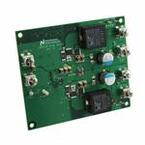
The LM5119EVAL evaluation board provides the design engineer with a fully functional dual output buck
converter, employing the LM5119 Dual Emulated Current Mode Synchronous Buck Controller. The
evaluation board is designed to provide both 10V and 5V outputs over an input range of 14V to 55V. Also
the evaluation board can be easily configured for a single 10V, 8A regulator.
2 Performance of the Evaluation Board
• Input Voltage Range: 14V to 55V
• Output Voltage: 10V (CH1), 5V (CH2)
• Output Current: 4A (CH1), 8A (CH2)
• Nominal Switching Frequency: 230 KHz
• Synchronous Buck Operation: Yes
• Diode Emulation Mode: Yes
• Hiccup Mode Overload Protection: Yes
• External VCC Sourcing: Yes
3 Powering and Loading Consideration
When applying power to the LM5119 evaluation board, certain precautions need to be followed. A
misconnection can damage the assembly.
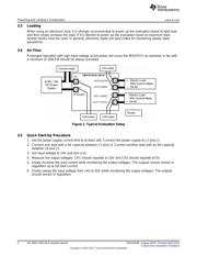
3.1 Proper Board Connection
The input connections are made to the J1 (VIN) and J2 (RTN/GND) connectors. The CH1 load is
connected to the J3 (OUT1+) and J4 (OUT1-/GND) and the CH2 load is connected to the J6 (OUT2+) and
J5 (OUT2-/GND). Be sure to choose the correct connector and wire size when attaching the source power
supply and the load.
3.2 Source Power
The power supply and cabling must present low impedance to the evaluation board. Insufficient cabling or
a high impedance power supply will droop during power supply application with the evaluation board
inrush current. If large enough, this droop will cause a chattering condition during power up. During power
down, insufficient cabling or a high impedance power supply will overshoot. This overshoot will cause a
non-monotonic decay on the output.
An additional external bulk input capacitor may be required unless the output voltage droop/overshoot of
the source power is less than 0.7V. In this board design, UVLO setting is conservative while UVLO
hysteresis setting is aggressive. Minimum input voltage can goes down with an aggressive design.
Minimum operating input voltage depends on the output voltage droop/overshoot of the source power
supply and the forced off-time of the LM5119. For complete design information, see the LM5119/LM5119Q
Wide Input Range Dual Synchronous Buck Controller Data Sheet (SNVS676).
All trademarks are the property of their respective owners.
1
SNVA444B–August 2010–Revised April 2013 AN-2065 LM5119 Evaluation Board
Submit Documentation Feedback
Copyright © 2010–2013, Texas Instruments Incorporated
Verzeichnis
- ・ Blockdiagramm on Seite 9
- ・ Anwendungsbereich on Seite 14
- ・ Elektrische Spezifikation on Seite 6