
herunterladen

User's Guide
SNOA496B–February 2008–Revised May 2013
AN-1743 LMH6552SDEVAL High Speed Differential
Amplifier Evaluation Board
1 General Description
The LMH6552SDEVAL evaluation board is designed to aid in the characterization of Texas Instruments
LMH6552 fully differential amplifier in an 8-pin LLP package. The LMH6552 is part of the LMH™ high-
speed amplifier family.
Use the evaluation board as a guide for high frequency layout and as a tool to aid in device testing and
characterization.
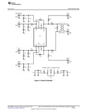
The evaluation board schematic is shown in Figure 1. For recommended for component values, see the
device-specific data sheets.
2 Basic Operation
The LMH6552SDEVAL evaluation board has been set up to provide maximum flexibility for evaluating TI’s
differential LMH6552 operational amplifier. The board supports fully differential operation as well as single-
ended to differential and single-ended to single-ended operation. For fully differential operation, use
resistors R
5
and R
6
to set the input impedance of the amplifier. Input resistance will be equal to 2*R
5
||
2*R
1
. Where R
5
= R
6
and R
1
= R
2
. In this mode resistors R
1
, R
2
, R
3
and R
4
set the gain of the amplifier.
Amplifier gain = R
F
/R
G
= R
4
/R
2
where R
1
= R
2
and R
3
= R
4
. For single-ended input mode of operation, the
input and termination resistance must be properly configured to give the correct gain and R
IN
. For
example, if a gain of 2 V/V is desired, R
5
= 28.7 Ω, R
1
= R
2
= 127 Ω, R
3
= R
4
= 275 Ω, and R
6
= 68.1 Ω,
which will make R
IN
= 50 Ω at the most positive node of R
5
looking into R
2
. For more details of single-
ended input mode calculations, see the LMH6552 1.5 GHz Fully Differential Amplifier Data Sheet
(SNOSAX9). Components R
7
, R
8
, C
6
, and C
7
should be used for AC-couple applications otherwise they
can be left empty.
For differential output applications, load R
12
and R
13
with the desired values to match the output load and
leave R
10
and R
11
empty.
If single-ended output is desired leave R
12
and R
13
empty and load R
10
, R
11
and an output transformer
such as the ADT4-1WT from mini circuits. The ADT4-1WT has a 4:1 impedance ratio (2:1 turns/voltage
ratio). This is particularly useful for interfacing to 50 Ω test equipment. When referencing the transformer
data sheet, the evaluation board has the primary windings on the output side of the evaluation board and
the amplifier is driving the secondary windings. This provides a step down transformation from the
differential amplifier output to the test equipment. The center-tapped secondary winding also allows a
differential to single ended conversion (Balun). The impedance seen by the differential amplifier = (R
10
+
R
11
+ R
L
*4), where R
L
is the impedance from pin 3 of the transformer to the load.
Pin 7 on the LMH6552 device is the enable (EN) pin that can be used to disable the device with an
external signal. For more details, see the LMH6552 1.5 GHz Fully Differential Amplifier Data Sheet
(SNOSAX9).
LMH is a trademark of Texas Instruments.
All other trademarks are the property of their respective owners.
1
SNOA496B–February 2008–Revised May 2013 AN-1743 LMH6552SDEVAL High Speed Differential Amplifier Evaluation
Board
Submit Documentation Feedback
Copyright © 2008–2013, Texas Instruments Incorporated
Verzeichnis
- ・ Blockdiagramm on Seite 3
- ・ Beschreibung der Funktionen on Seite 1
- ・ Anwendungsbereich on Seite 5