

herunterladen

User's Guide
SNWA007A–March 2008–Revised April 2013
AN-1804 LMV225/LMV228 DSBGA
Evaluation Board
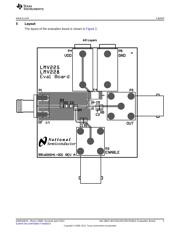
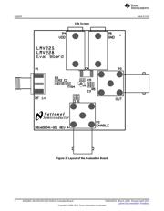
1 General Description
This board can be used to evaluate the Texas Instruments LMV225 and LMV228 RF detectors. These
logarithmic power detectors are intended for use in CDMA and WCDMA applications. They have a 30 dB
dynamic range and an RF frequency range from 450 MHz to 2 GHz. The LMV228 is designed to be used
in combination with a directional coupler, while the LMV225 detector is especially suited for power
measurements via a high-resistive tap as well as directional coupler. The LMV225 and LMV228 have an
integrated filter for low-ripple average power detection of CDMA signals. Additional filtering can be applied
using a single external capacitor.
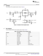
2 Basic Operation
The LMV225 and LMV228 provide an accurate temperature and supply compensated DC output voltage
that relates linearly to the applied RF input power in dBm. The single supply, ranging from 2.7V to 5.5V,
can be applied through connectors P
4
and P
5
. The signal applied to connector P
2
puts the detector in an
active or a shutdown mode. The detector is active for Enable = HI, otherwise it is in a low power
consumption shutdown mode. The RF signal is applied through connector P
1
, while the output voltage is
measured through connector P
3
.
2.1 Input
The LMV225 has an RF power detection range from −30 dBm to 0 dBm and is designed for direct use in
combination with resistive taps. The LMV228 has a detection range from −15 dBm to 15 dBm and are
intended for use in combination with a directional coupler. All three detectors have an input impedance of
50Ω. Details about the configuration can be found in the devices' data sheet.
2.2 Output
The output voltage range is typically 0.2V to 2V and can be scaled down to meet ADC input range
requirements (both LMV225 and LMV228). Since the LMV225 and LMV228 have a current controlled
output, the voltage range can be adjusted by changing the output resistance. To change this a resistor
needs to be placed in R
5
. The output impedance of the detector (typical 19.8 kΩ) together with the resistor
R
5
translates the current into a voltage. The value of resistor R
5
determines the exact scaling. A value of
19.8 kΩ, for example, divides the output voltage range by half. Besides scaling the output voltage, the
output ripple can be reduced by lowpass filtering. This can be realized with capacitor C
3
. Further details
can be found in the applications information section in the devices' data sheet..
All trademarks are the property of their respective owners.
1
SNWA007A–March 2008–Revised April 2013 AN-1804 LMV225/LMV228 DSBGA Evaluation Board
Submit Documentation Feedback
Copyright © 2008–2013, Texas Instruments Incorporated
Verzeichnis