
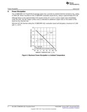

herunterladen

User's Guide
SNVA204B–January 2007–Revised April 2013
AN-1560 LP38852MR-ADJ Evaluation Board
1 Introduction
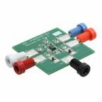
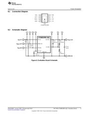
This board is designed to allow the evaluation of the LP38852MR-ADJ voltage regulator. Each board is
assembled and tested in the factory. This evaluation board has the SO PowerPAD-8 package mounted,
and the output voltage is set to 1.20V.
2 General Description
The LP38852 is a dual-rail adjustable LDO linear regulator capable of suppling up to 1.5A of output
current, and incorporates an Enable function as well as a Soft-Start function.
The device has been designed to work with 10 µF input and output ceramic capacitors, and 1µF bias
capacitor. Footprints areas for C
IN
and C
OUT
will allow for a variety of sizes.
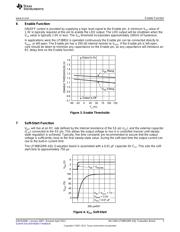
3 Operation
The input voltage, applied between V
IN
and GND, should be at least 1.0V greater than V
OUT
and no greater
than the applied V
BIAS
voltage.
The bias voltage, applied between V
BIAS
and GND should be above the minimum bias voltage of 3.0V, and
no more than the maximum of 5.5V.
Loads can be connected to V
OUT
with reference to GND.
V
OUT
and V
IN
test points are provided on the board to allow accurate measurements directly onto the input
and output pins of the device, eliminating any voltage drop on the PCB traces or connecting wires to the
load.
4 Setting V
OUT
The output voltage is set using the external resistive divider R1 and R2. The output voltage is given by the
formula:
V
OUT
= V
ADJ
x (1 + (R1 / R2)) (1)
It is recommended that the values selected for R1 and R2 are such that the parallel value is less than 10
kΩ. This is to prevent internal parasitic capacitances on the ADJ pin from interfering with the F
Z
pole set
by R1 and C
FF
.
The LP38852MR-ADJ Evaluation board is assembled with a 1.40 kΩ ±1% resistor for R1, and a 1.00 kΩ
±1% resistor for R2. This sets V
OUT
to 1.20V.
5 Selecting C
FF
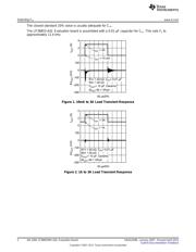
A capacitor placed across the gain resistor R1 will provide additional phase margin to improve load
transient response of the device. This capacitor, C
FF
, in parallel with R1, will form a zero in the loop
response given by the formula:
F
Z
= (1 / (2 x π x C
FF
x R1) ) (2)
The value for C
FF
should be selected to set a zero frequency (F
Z
) between 10 kHz and 15 kHz using the
formula:
C
FF
= 1 / (2 x π x F
Z
x R1) (3)
All trademarks are the property of their respective owners.
1
SNVA204B–January 2007–Revised April 2013 AN-1560 LP38852MR-ADJ Evaluation Board
Submit Documentation Feedback
Copyright © 2007–2013, Texas Instruments Incorporated
Verzeichnis
- ・ Blockdiagramm on Seite 5
- ・ Beschreibung der Funktionen on Seite 1
- ・ Anwendungsbereich on Seite 8