
herunterladen
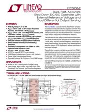
LTC3838-2
1
38382fa
For more information www.linear.com/3838-2
Typical applicaTion
FeaTures DescripTion
Dual, Fast, Accurate
Step-Down DC/DC Controller with
External Refer
ence Voltage and
Dual Differential Output Sensing
The LTC
®
3838-2 is a dual-channel, PolyPhase
®
synchro-
nous step-down
DC/DC switching regulator controller. Two
independent channels drive all N-channel power MOSFETs.
The two channels can also be combined into a multiphase
single output configuration with external reference.
The controlled on-time, valley current mode control architec
-
ture allows
for
not only fast response to transients without
a clock delay, but also constant frequency switching at a
steady-load condition. Its proprietary load-release transient
detection feature (DTR) significantly reduces overshoot at
low output voltages.
The switching frequency can be programmed from 200kHz
to 2MHz with an external resistor, and can be synchronized
to an external clock. Very low t
ON
and t
OFF
times allow for near
0% and near 100% duty cycles, respectively. Voltage track-
ing soft
start
-up and multiple safety features are provided.
See Table 1 for a comparison of LTC3838, LTC3838-1 and
LTC3838-2.
L, LT, LTC, LTM, PolyPhase, OPTI-LOOP, µModule, Linear Technology and the Linear logo are
registered trademarks of Linear Technology Corporation. All other trademarks are the property
of their respective owners. Protected by U.S. Patents, including 5481178, 5847554, 6580258,
6304066, 6476589, 6774611.
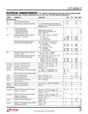
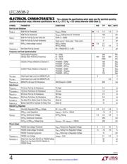
1.2V/15A and 0.8V to 2.5V/15A, 350kHz Step-Down Converter (See Figure 16 for Complete Design)
applicaTions
n
Wide V
IN
Range: 4.5V to 38V
n
V
OUT1
: 0.6V to 5.5V, ±0.67% Output Regulation
Accuracy, with Internal 0.6V V
REFERENCE
n
V
OUT2
: 0.4V to 5.5V, ±4mV Regulation Accuracy, with
Differential External V
REFERENCE
Sensing
n
Differential Remote Output Sensing; Up to ±500mV
(V
OUT1
) and ±200mV (V
OUT2
) Ground Deviations
n
Fast Load Transient Response Without Clock Delay
n
Detect Transient Release (DTR) Reduces V
OUT
Overshoot
n
Frequency Programmable from 200kHz to 2MHz,
Synchronizable to External Clock
n
t
ON(MIN)
= 30ns, t
OFF(MIN)
= 90ns
n
R
SENSE
or Inductor DCR Current Sensing
n
Overvoltage Protection and Current Limit Foldback
n
Power Good Output Voltage Monitor
n
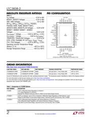
Thermally Enhanced 38-Pin (5mm × 7mm) QFN Package
n
Power for ASICs with Dynamic Voltage Scaling
n
Low Voltage, High Current, High Step-Down Ratio
Converters That Demand Tight Transient Regulation
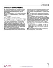
Efficiency/Power Loss
115k
SENSE1
–
SENSE1
+
SENSE2
–
SENSE2
+
V
IN
BOOST1
DRV
CC1
TG1
BG1
PGND
0.4V TO
1.25V
BG2
EXTV
REF2
DRV
CC2
V
OUTSENSE1
+
V
OUTSENSE1
–
TRACK/SS1
ITH1
V
DFB2
+
V
DFB2
–
TRACK/SS2
ITH2
4.7µF
V
OUT2
0.8V TO 2.5V
15A
V
IN
4.5V TO 38V
V
OUT1
1.2V
15A
0.1µF 0.1µF
330µF
×2
330µF
×2
10k
10k
20k
20k
10k
0.56µH
0.56µH
38382 TA01a
RT
SGND
EXTV
CC
RUN1
MODE/PLLIN
CLKOUT
PHASMD
RUN2
SW1
BOOST2
LTC3838-2
TG2
INTV
CC
SW2
+
+
LOAD CURRENT (A)
0.1
40
EFFICIENCY (%)
POWER LOSS (W)
80
90
100
1
EFFICIENCY
10
38382 TA01b
70
60
50
0
1.5
2.0
2.5
1.0
0.5
V
IN
= 12V
V
OUT
= 1.2V
FORCED CONTINUOUS MODE
DISCONTINUOUS MODE
POWER
LOSS
Verzeichnis
- ・ Konfiguration des Pinbelegungsdiagramms on Seite 17
- ・ Abmessungen des Paketumrisses on Seite 54
- ・ Paket-Footprint-Pad-Layout on Seite 54
- ・ Typisches Anwendungsschaltbild on Seite 11 Seite 14 Seite 15 Seite 16 Seite 17
- ・ Technische Daten on Seite 5
- ・ Anwendungsbereich on Seite 11 Seite 16 Seite 26
- ・ Elektrische Spezifikation on Seite 10 Seite 16 Seite 21 Seite 28 Seite 31