
herunterladen
Click here for an overview of the wireless
components used in a typical radio
transceiver.
Maxim > Design Support > Technical Documents > Application Notes > Wireless and RF > APP 1962
Keywords: rf, rfic, wireless, td-scdma, evm, acir, acs, rf ics, rfics
APPLICATION NOTE 1962
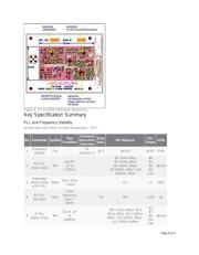
TD-SCDMA Reference Design V1.0
Mar 26, 2003
Abstract: This application note presents Maxim's TD-SCDMA reference design V1.0. TD-SCDMA is the
Chinese Third Generation (3G) standard. China's government has allocated 3 frequency bands:
1880~1920MHz, 2010~2025MHz, and 2300~2400MHz. Maxim's TD-SCDMA reference design 1.0 focuses
on the 2015~2025MHz band, which is the first frequency band for TD-SCDMA. Included are the block
diagram, test results, PCB layout outlines and measured performance.
Additional Information:
Wireless Product Line Page
Quick View Data Sheet for the MAX2306, MAX2308, MAX2309
Quick View Data Sheet for the MAX2361, MAX2363, MAX2365
Quick View Data Sheet for the MAX2470, MAX2471
Applications Technical Support
Introduction
TD-SCDMA (time division synchronous code division multiple
access) is one of three 3G standards. The Chinese government
recently (2002-10) allocated 155MHz of bandwidth for this standard. The TD-SCDMA standard now has
three frequency bands: 1880~1920MHz, 2010~2025MHz, and 2300~2400MHz. Maxim currently produces
many RF ICs that will operate in these frequency bands, and support the new standard, as is evidenced
by the performance documented here.
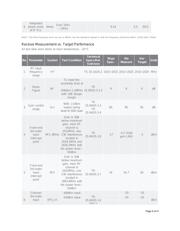
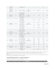
This document presents the performance of Maxim's TD-SCDMA V1.0 (version one) reference design,
and discusses the design specification and testing results. The full performance specification for the radio
is documented by 3GPP (Third Generation Partnership Project) (www.3gpp.org) in specification 25.945
V5.0.0.
TD-SCDMA Reference Design Description
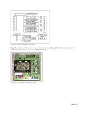
The Maxim TD-SCDMA reference design Version 1.0 is a single-mode, single-band transceiver intended
to support the TD-SCDMA standard. All active ICs in this reference design are from Maxim, except one
PLL required due to fast lock-time requirements. This transceiver operates from a single 2.9V to 3.6V
supply, drawing about 73mA in receive mode and about 373mA in transmit mode, while delivering
+16dBm at antenna port. This reference design offers a complete handset transceiver design, providing
the highest integration available in the industry.
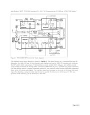
The complete radio is designed to fit a single-sided 40mm x 65mm PCB. The radio transceiver block
diagram is shown in Figure 1. This transceiver is designed to meet the TD-SCDMA handset radio
Page 1 of 41