
herunterladen

Maxim > Design Support > Technical Documents > Reference Designs > A/D and D/A Conversion/Sampling Circuits > APP 2398
Maxim > Design Support > Technical Documents > Reference Designs > Amplifier and Comparator Circuits > APP 2398
Maxim > Design Support > Technical Documents > Reference Designs > Automotive > APP 2398
Keywords: 3V DACs, level shifting, +/-10V, 10V, 3V output, industrial DAC, bipolar, resistor networks, gain
setting resistor, amplifier, op amp, digital pot
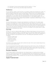
REFERENCE DESIGN 2398 INCLUDES: Tested Circuit Schematic Description Test Data
3V DACs Used in ±10V Applications
Sep 29, 2003
Abstract: Many modern systems have the majority of their electronics powered by 3.3V or lower, but must
drive external loads with ±10V, a range that is still very common in industrial applications. There are digital
to analog converters (DACs) available that can drive loads with ±10V swings, but there are reasons to use
a 3.3V DAC and amplify the output voltage up to ±10V.
Introduction
Modern logic systems that use 3.3V supplies must sometimes run industrial applications which require
voltages of ±10V, such as PLC, transmitters, and motor control. One solution is to choose a digital to
analog converter (DAC) that can deliver ±10V swings, but an alternative is to use a 3.3V DAC and amplify
the output voltage up to ±10V. Examples:
3.3V DACs may have higher levels of desired logic integration than their ±10V counterparts.
3.3V DACs tend to have higher speed logic interfaces, freeing the microcontroller for other tasks.
The DAC may be integrated into a larger chip, powered from 3.3V (such as a microcontroller) and not
capable of ±10V output swings.
The external loads may have output current drive requirements or capacitive loads that cannot be
handled by the 3.3V ±10V DAC.
Circuit Overview
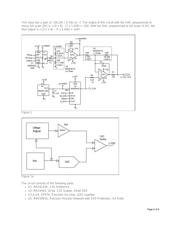
The circuit's block diagram is shown in Figure 1a. It consists of five main blocks: DAC, Reference, Offset
Adjust, Reference Buffer, and Output Buffer.
The DAC provides the digital-code-to-voltage translation, relative to the Reference. Offset Adjust provides
the ability to offset the DAC's unipolar transfer function to create a bipolar output and the ability to
calibrate the 0V output point. The Reference Buffer provides load isolation for the Reference and the Offset
Adjust. The Output Buffer sums in the offset adjustments and provides the required gain to increase the
output swing to the desired magnitude. Additionally the Output Buffer provides the ability to drive a load.
Circuit Description
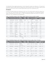
The circuit in Figure 1 and Figure 1a illustrates how a 3.3V powered 16-bit DAC can be buffered to
achieve output swings of ±10V. The DAC (U2) has a 0 to 2.5V output range and is connected to the non-
inverting input of op amp U3. This input has a non-inverting gain of (1 + 26.25k / 3.75k) or 8. The inverting
input of the op amp is connected to +1.429V created by the reference and the resistor divider network.
Page 1 of 5
Verzeichnis
- ・ Blockdiagramm on Seite 1
- ・ Anwendungsbereich on Seite 1