
herunterladen
Ordering Information and Selector Guide appears at end of
data sheet.
19-6355; Rev 6; 12/17
General Description
The MAX6070/MAX6071 offer a very low noise and
low-drift voltage reference in a small 6-pin SOT23 package.
These devices provide a 1/f noise voltage of only
4.8µV
P-P
at an output voltage of 2.5V, with a temperature
drift of 6ppm/NC (max). The devices consume 150FA of
supply current and can sink and source up to 10mA of load
current. The low-drift and low-noise specifications enable
enhanced system accuracy, making these devices ideal
for high-precision industrial applications. The MAX6070
offers a noise filter option for wideband applications.
The devices are available in a 6-pin SOT23 package and
are specified over the extended industrial temperature
range of -40NC to +125NC. The 2.5V options are also
available in a 6-bump 0.78mm x 1.41mm wafer-level
package (WLP).
Applications
● High-Accuracy Industrial and Process Control
● Precision Instrumentation
● High-Resolution ADCs and DACs
● Precision Current Sources
Benets and Features
● 6-Pin SOT23 Package Reduces System Board Space
● Stable Performance Over Temperature and Time
Improves System Accuracy
• High ±0.04% Initial Accuracy
• Low 1.5ppm/°C (typ), 6ppm/°C (max) Temperature
Drift
• Low 4.8μV
P-P
Noise (0.1Hz to 10Hz) at 2.5V
• Low 200mV Dropout Voltage
• High 85dB Ripple Rejection
● Low 150μA Supply Current Reduces Power
Consumption
● Filter Option Lowers High-Frequency Noise
● Output Options: 1.25V, 1.8V, 2.048V, 2.5V, 3.0V,
3.3V, 4.096V, and 5.0V Cover Common Voltage
Levels for a Wide Variety of Applications
● 0.78mm x 1.41mm WLP with 0.35mm Bump Spacing
● AEC-Q100 Qualified (Refer to Ordering Information)
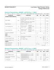
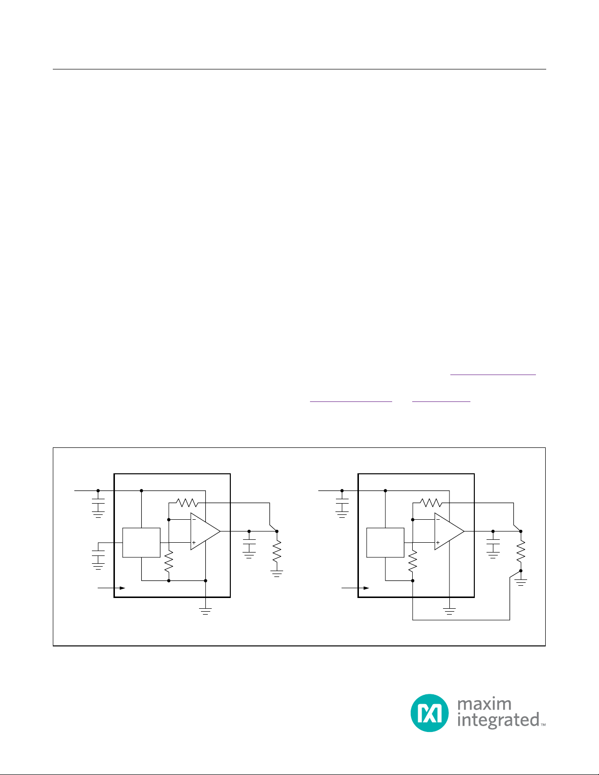
BANDGAP
VOLTAGE
REFERENCE
GND
0.1µF
0.1µF
0.1µF
IN
FILTER
EN
SHUTDOWN
CONTROL
V
IN
R
L
OUTF
OUTS
V
OUT
BANDGAP
VOLTAGE
REFERENCE
GNDFGNDS
0.1µF
0.1µF
IN
EN
SHUTDOWN
CONTROL
V
IN
R
L
OUTF
OUTS
V
OUT
MAX6070 MAX6071
Typical Operating Circuits
MAX6070/MAX6071 Low-Noise, High-Precision Series
Voltage References
EVALUATION KIT AVAILABLE
Verzeichnis
- ・ Konfiguration des Pinbelegungsdiagramms on Seite 19
- ・ Abmessungen des Paketumrisses on Seite 24
- ・ Teilenummerierungssystem on Seite 1 Seite 24
- ・ Typisches Anwendungsschaltbild on Seite 1
- ・ Beschreibung der Funktionen on Seite 1
- ・ Technische Daten on Seite 12
- ・ Anwendungsbereich on Seite 1 Seite 21
- ・ Elektrische Spezifikation on Seite 3 Seite 4 Seite 5 Seite 6 Seite 7