


herunterladen

Maxim > Design Support > Technical Documents > Reference Designs > Power-Supply Circuits > APP 5448
Keywords: FPGA, Xilinx, power module, Kintex, 7 series, reference design, point of load regulator, power supply, POL
REFERENCE DESIGN 5448 INCLUDES: Tested Circuit Schematic BOM
Kintex-7 Series Power Module
By: Takahiro Hayashi
Murali Krushna
Jul 17, 2012
Abstract: This reference design enables a complete power-supply solution for powering Xilinx® Kintex®-7 series field-programmable gate
array (FPGA) using Maxim's power-supply solutions.
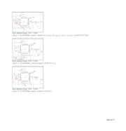
This fully tested reference design provides a complete power-supply solution for powering a typical Xilinx Kintex-7 series field-
programmable gate array (FPGA) using Maxim's power-supply solutions. The Kintex-7 (7K325T FPGA application) requires eight distinct
power supply rails as follows:
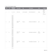
Design Description
FPGA Rail Input Voltage Output Voltage Current Maxim Solution
V
CCINT
, V
CCBRAM
12V 1V 6A MAX8686
V
CCAUX
, V
CCAUX_IO
, V
CCO
, V
CCADC
, MGTAVCCAUX 12V 1.8V 6A MAX8686
MGTAVCC 12V 1V 6A MAX8686
V
CC0
12V 3.3V 8A MAX8686
V
CC0
12V 2.5V 8A MAX8686
V
CC0
12V 1.5V/1.35V 4A MAX8654
MGTAVTT, MGTAVTTRCAL 12V 1.2V 4A MAX8654
V
CCAUX_IO
12V 2V 2A MAX15041
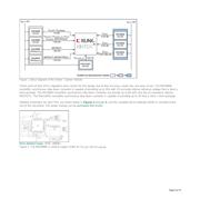
This reference design provides the required eight power rails using five MAX8686 synchronous pulse-width modulation (PWM) step-down
regulators, two MAX8654 high-efficiency switching regulators, and the MAX15041 low-cost synchronous DC-DC converter with internal
switches. These devices can be sequenced at power-up, as indicated in Figure 1.
Page 1 of 14