

herunterladen
© Semiconductor Components Industries, LLC, 2016
July, 2016 − Rev. 11
1 Publication Order Number:
MC10EL33/D
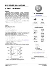
MC10EL33, MC100EL33
5 V ECL ÷4 Divider
Description
The MC10EL/100EL33 is an integrated ÷4 divider. The differential
clock inputs and the V
BB
allow a differential, single-ended or AC coupled
interface to the device. The V
BB
pin, an internally generated voltage
supply, is available to this device only. For single-ended input conditions,
the unused differential input is connected to V
BB
as a switching reference
voltage. V
BB
may also rebias AC coupled inputs. When used, decouple
V
BB
and V
CC
via a 0.01 mF capacitor and limit current sourcing or sinking
to 0.5 mA. When not used, V
BB
should be left open.
The reset pin is asynchronous and is asserted on the rising edge. Upon
power-up, the internal flip-flops will attain a random state; the reset allows
for the synchronization of multiple EL33’s in a system.
The 100 Series contains temperature compensation.
Features
• 650 ps Propagation Delay
• 4.0 GHz Toggle Frequency
• ESD Protection:
♦ > 1 kV Human Body Model
♦ > 100 V Machine Model
• PECL Mode Operating Range: V
CC
= 4.2 V to 5.7 V with V
EE
= 0 V
• NECL Mode Operating Range: V
CC
= 0 V with V
EE
= −4.2 V to −5.7 V
• Internal Input Pulldown Resistors on CLK(s) and R.
• Meets or Exceeds JEDEC Spec EIA/JESD78 IC Latchup Test
• Moisture Sensitivity:
♦ Level 1 for SOIC−8 NB
♦ Level 3 for TSSOP−8
♦ For Additional Information, see Application Note AND8003/D
• Flammability Rating: UL 94 V−0 @ 0.125 in,
Oxygen Index: 28 to 34
• Transistor Count = 95 Devices
• These Devices are Pb-Free, Halogen Free and are RoHS Compliant
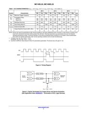
Figure 1. Logic Diagram and Pinout Assignment
4
3
1
2
5
6
7
8
Q
V
EE
V
CC
QCLK
V
BB
R
÷4
Reset
CLK
*For additional marking information, refer to
Application Note AND8002/D
.
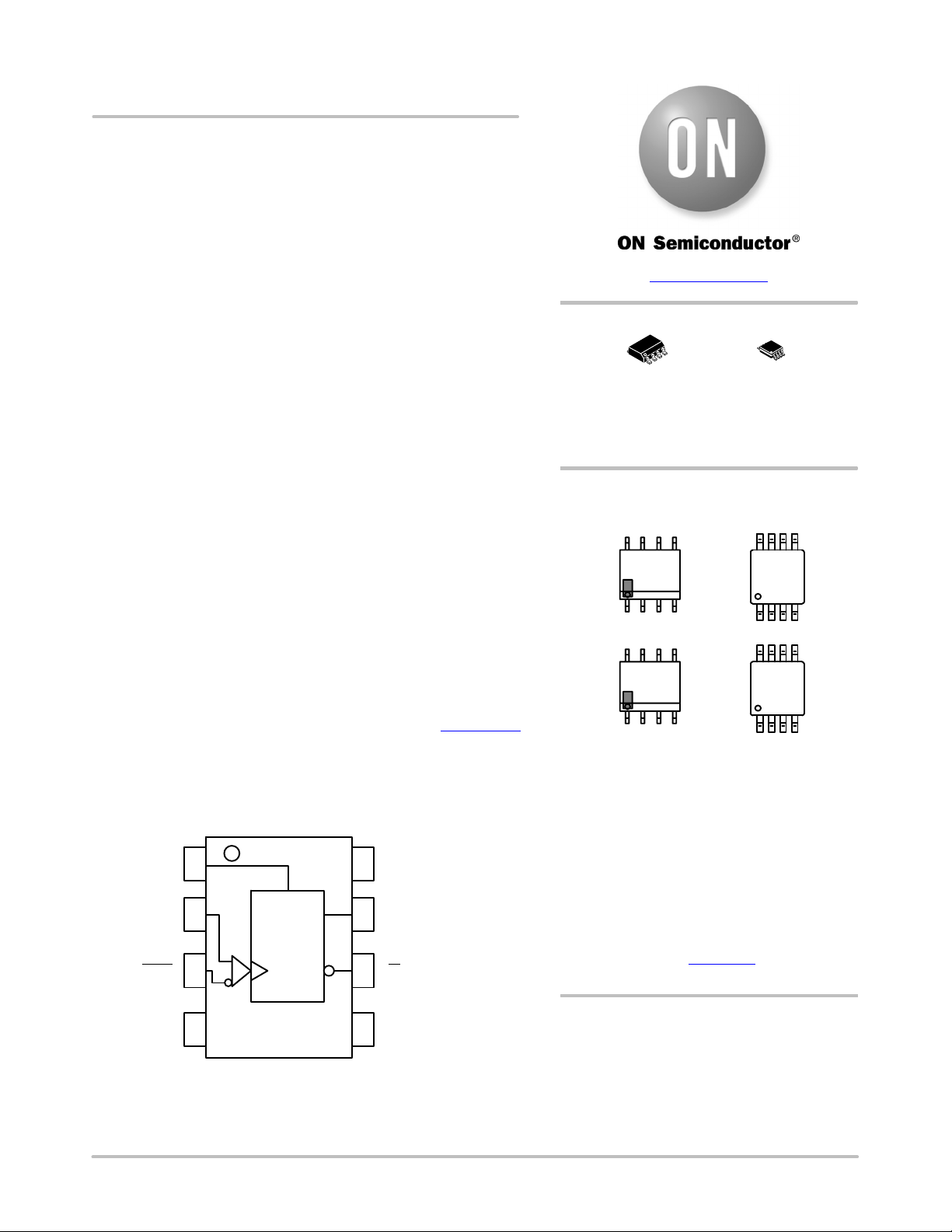
MARKING DIAGRAMS*
KL33
ALYWG
G
SOIC−8 NB
D SUFFIX
CASE 751−05
1
8
TSSOP−8
DT SUFFIX
CASE 948R−02
1
8
1
8
ORDERING INFORMATION
www.onsemi.com
KEL33
ALYW
G
1
8
HL33
ALYWG
G
1
8
HEL33
ALYW
G
1
8
(Note: Microdot may be in either location)
H = MC10
K = MC100
A = Assembly Location
L = Wafer Lot
Y = Year
W = Work Week
G = Pb-Free Package
SOIC−8 NB TSSOP−8
See detailed ordering and shipping information on page 6 of
this data sheet.
Verzeichnis
- ・ Konfiguration des Pinbelegungsdiagramms on Seite 2
- ・ Abmessungen des Paketumrisses on Seite 7 Seite 8
- ・ Paket-Footprint-Pad-Layout on Seite 7
- ・ Teilenummerierungssystem on Seite 1 Seite 6 Seite 8
- ・ Markierungsinformationen on Seite 1 Seite 6 Seite 8
- ・ Typisches Anwendungsschaltbild on Seite 1
- ・ Technische Daten on Seite 6
- ・ Teilenummernliste on Seite 2