
herunterladen
© Semiconductor Components Industries, LLC, 2012
August, 2012 − Rev. 1
1 Publication Order Number:
EVBUM2131/D
NCP1230GEVB
NCP1230 90 Watt, Universal
Input Adapter Power Supply
Evaluation Board User's
Manual
General Description
The NCP1230 implements a standard current mode
control architecture. It’s an ideal candidate for applications
where a low parts count is a key parameter, particularly in
low cost adapter power supplies. The NCP1230 combines a
low standby power mode with an event management scheme
that will disable a PFC circuit during Standby, thus reducing
the no load power consumption. The 90 W Evaluation
Board demonstrates the wide range of features found on the
NCP1230 controller.
The NCP1230 has a PFC_Vcc output pin which provides
Vcc power for a PFC controller, or other circuitry. The
PFC_Vcc pin is enabled when the output of the power
supply is up and in regulation. In the event that there is an
output fault, the PFC_Vcc pin is turned off, disabling the
PFC controller, reducing the stress on the PFC
semiconductors.
In addition to excellent no load power consumption, the
NCP1230 provides an internal latching function that can be
used for over voltage protection by pulling the CS pin above
3.0 V.
Features
• Current−Mode Control
• Lossless Startup Circuit
• Operation Over the Universal Input Range
• Direct Connection to PFC Controller
• Low Standby
• Overvoltage Protection
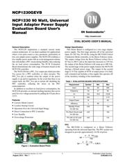
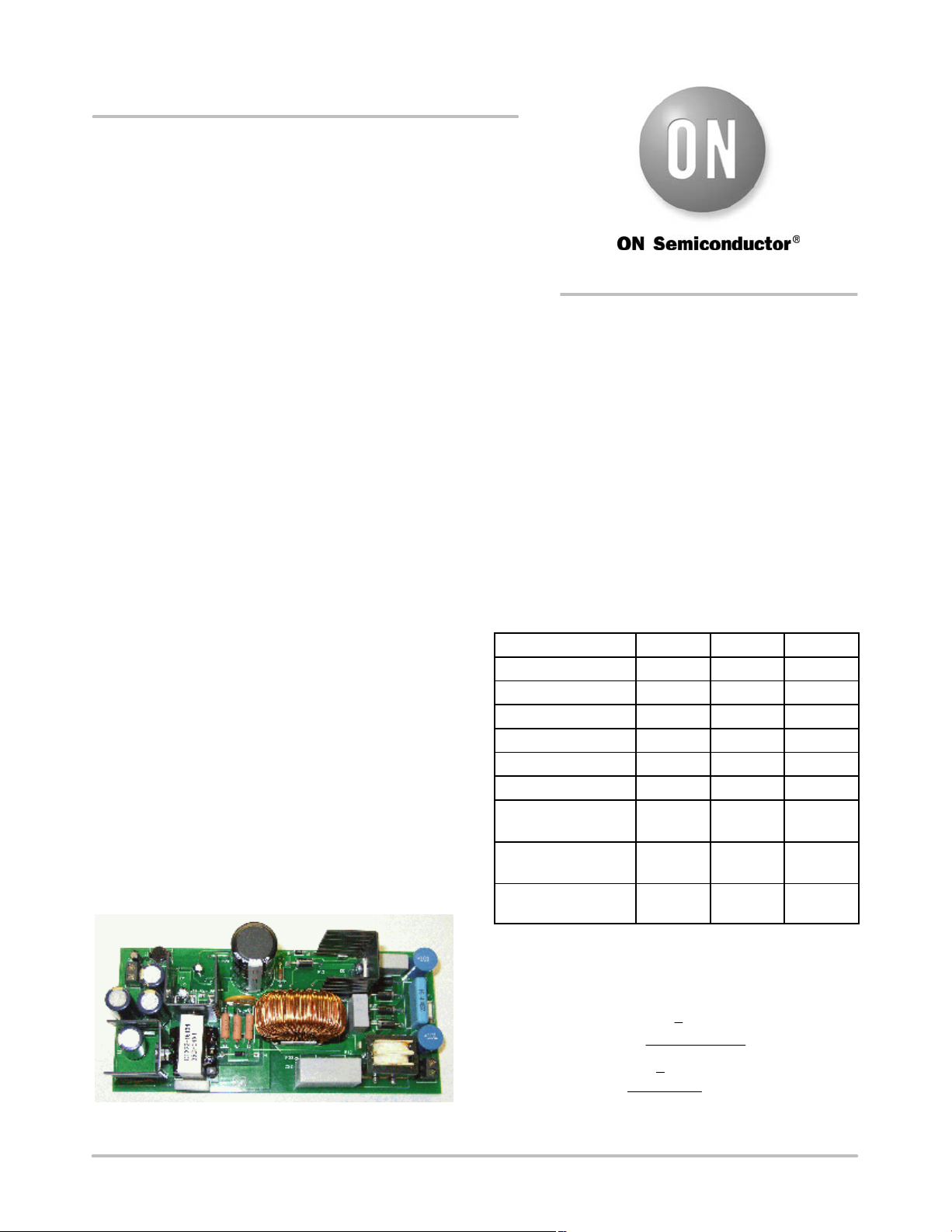
Figure 1. Evaluation Board Photo
Design Specification
This Demo Board is configured as a two stage adapter
power supply. The first stage operates off of the universal
input, 85−265 Vac, 50−60 Hz, using the MC33260 Critical
Conduction Mode controller, in the Boost Follower mode.
The output voltage from the Boost Follower (when Vin is
85 Vac) is 200 V and as the input line increases to 230 Vac
the output of the Boost Follower will ramp up to 400 Vdc.
The second stage of the power supply features the NCP1230
driving a flyback power stage. The output of the second
stage is 19 Vdc capable of 90 W of output power. It is fully
self−contained and includes a bias supply that operates off
of the Auxiliary winding of the transformer.
Table 1. EVALUATION BOARD SPECIFICATIONS
Requirement Symbol Min Max
Input Vac 85 265
Frequency Hz 47 63
Vo Vdc 18.6 19.38
Io Adc − 4.74
Output Power W − 90
efficiency
h
80 −
Standby Power
Vin 230 Vac
mW − 150
Pin Short Circuit Load
Vin 230 Vac
mW 100
Pin with 0.5 W Load
Vin 230 Vac
mW − 0.8
PFC
The MC33260 is configured as a Boost Follower
operating from the universal input line. The PFC section was
designed to provide approximately 116 W of power.
Ipk +
2· 2
Ǹ
·Pin
max
Vac
Ipk +
2· 2
Ǹ
·116
85
+ 3.86 A
http://onsemi.com
EVAL BOARD USER’S MANUAL
Verzeichnis