
herunterladen
© Semiconductor Components Industries, LLC, 2015
June, 2015 − Rev. 22
1 Publication Order Number:
NCP500/D
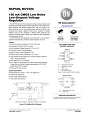
NCP500, NCV500
150 mA CMOS Low Noise
Low-Dropout Voltage
Regulator
The NCP500 series of fixed output low dropout linear regulators are
designed for portable battery powered applications which require low
noise operation, fast enable response time, and low dropout. The
device achieves its low noise performance without the need of an
external noise bypass capacitor. Each device contains a voltage
reference unit, an error amplifier, a PMOS power transistor, and
resistors for setting output voltage, and current limit and temperature
limit protection circuits.
The NCP500 has been designed to be used with low cost ceramic
capacitors and requires a minimum output capacitor of 1.0 mF.
Features
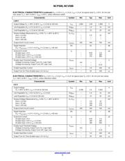
• Ultra−Low Dropout Voltage of 170 mV at 150 mA
• Fast Enable Turn−On Time of 20 msec
• Wide Operating Voltage Range of 1.8 V to 6.0 V
• Excellent Line and Load Regulation
• High Accuracy Output Voltage of 2.5%
• Enable Can Be Driven Directly by 1.0 V Logic
• Typical RMS Noise Voltage 50 mV with No Bypass Capacitor
(BW = 10 Hz to 100 kHz)
• Very Small DFN 2x2.2 Package
• NCV Prefix for Automotive and Other Applications Requiring
Unique Site and Control Change Requirements; AEC−Q100
Qualified and PPAP Capable
• These are Pb−Free Devices
Typical Applications
• Noise Sensitive Circuits − VCO’s, RF Stages, etc.
• SMPS Post−Regulation
• Hand−Held Instrumentation
• Camcorders and Cameras
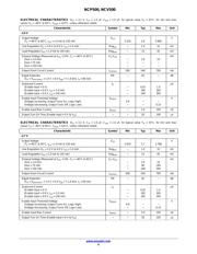
Driver w/
Current
Limit
V
in
V
out
Thermal
Shutdown
Enable
GND
OFF
ON
1 (3)
3 (1)
5 (4)
2 (2, 5)
Figure 1. Simplified Block Diagram
NOTE: Pin numbers in parenthesis indicate DFN package.
See detailed ordering and shipping information in the package
dimensions section on page 16 of this data sheet.
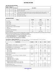
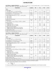
ORDERING INFORMATION
TSOP−5
SN SUFFIX
CASE 483
1
5
PIN CONNECTIONS AND
MARKING DIAGRAMS
1
3
N/C
V
in
2GND
Enable
4
V
out
5
xxx = Specific Device Code
A = Assembly Location
Y = Year
W = Work Week
G = Pb−Free Package
(Note: Microdot may be in either location)
(Top View)
TSOP−5
DFN 2x2.2 MM
SQL SUFFIX
CASE 506BA
1
3
N/C
V
in
2
GND
Enable
4
V
out
5
6
GND
(Top View)
www.onsemi.com
xxM
xxxAYWG
G
DFN 2x2.2 mm
xx = Specific Device Code
M = Date Code
1
6
Verzeichnis
- ・ Konfiguration des Pinbelegungsdiagramms on Seite 1
- ・ Abmessungen des Paketumrisses on Seite 17 Seite 18
- ・ Paket-Footprint-Pad-Layout on Seite 17 Seite 18
- ・ Teilenummerierungssystem on Seite 1 Seite 16 Seite 18
- ・ Markierungsinformationen on Seite 1 Seite 16 Seite 18
- ・ Blockdiagramm on Seite 1
- ・ Typisches Anwendungsschaltbild on Seite 1 Seite 13
- ・ Beschreibung der Funktionen on Seite 2
- ・ Technische Daten on Seite 16
- ・ Anwendungsbereich on Seite 1 Seite 12 Seite 16
- ・ Elektrische Spezifikation on Seite 2 Seite 3 Seite 4 Seite 5 Seite 6
- ・ Teilenummernliste on Seite 2