
herunterladen
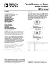
Precision Micropower, Low Dropout
Voltage References
REF19x Series
Rev. H
Information furnished by Analog Devices is believed to be accurate and reliable.
However, no responsibility is assumed by Analog Devices for its use, nor for any
infringements of patents or other rights of third parties that may result from its use.
Specifications subject to change without notice. No license is granted by implication
or otherwise under any patent or patent rights of Analog Devices. Trademarks and
registered trademarks are the property of their respective owners.
One Technology Way, P.O. Box 9106, Norwood, MA 02062-9106, U.S.A.
Tel: 781.329.4700 www.analog.com
Fax: 781.461.3113 © 2005 Analog Devices, Inc. All rights reserved.
FEATURES
Initial accuracy: ±2 mV max
Temperature coefficient: 5 ppm/°C max
Low supply current: 45 μA max
Sleep mode: 15 μA max
Low dropout voltage
Load regulation: 4 ppm/mA
Line regulation: 4 ppm/V
High output current: 30 mA
Short-circuit protection
APPLICATIONS
Portable instruments
A/D and D/A converters
Smart sensors
Solar-powered applications
Loop-current-powered instruments
GENERAL DESCRIPTION
The REF19x series precision band gap voltage references use a
patented temperature drift curvature correction circuit and
laser trimming of highly stable, thin-film resistors to achieve a
very low temperature coefficient and high initial accuracy.
The REF19x series is made up of micropower, low dropout
voltage (LDV) devices, providing stable output voltage from
supplies as low as 100 mV above the output voltage and
consuming less than 45 μA of supply current. In sleep mode,
which is enabled by applying a low TTL or CMOS level to the
SLEEP
pin, the output is turned off and supply current is
further reduced to less than 15 μA.
The REF19x series references are specified over the extended
industrial temperature range (−40°C to +85°C) with typical
performance specifications over −40°C to +125°C for
applications, such as automotive.
All electrical grades are available in an 8-lead SOIC package; the
PDIP and TSSOP packages are available only in the lowest
electrical grade. Products are also available in die form.
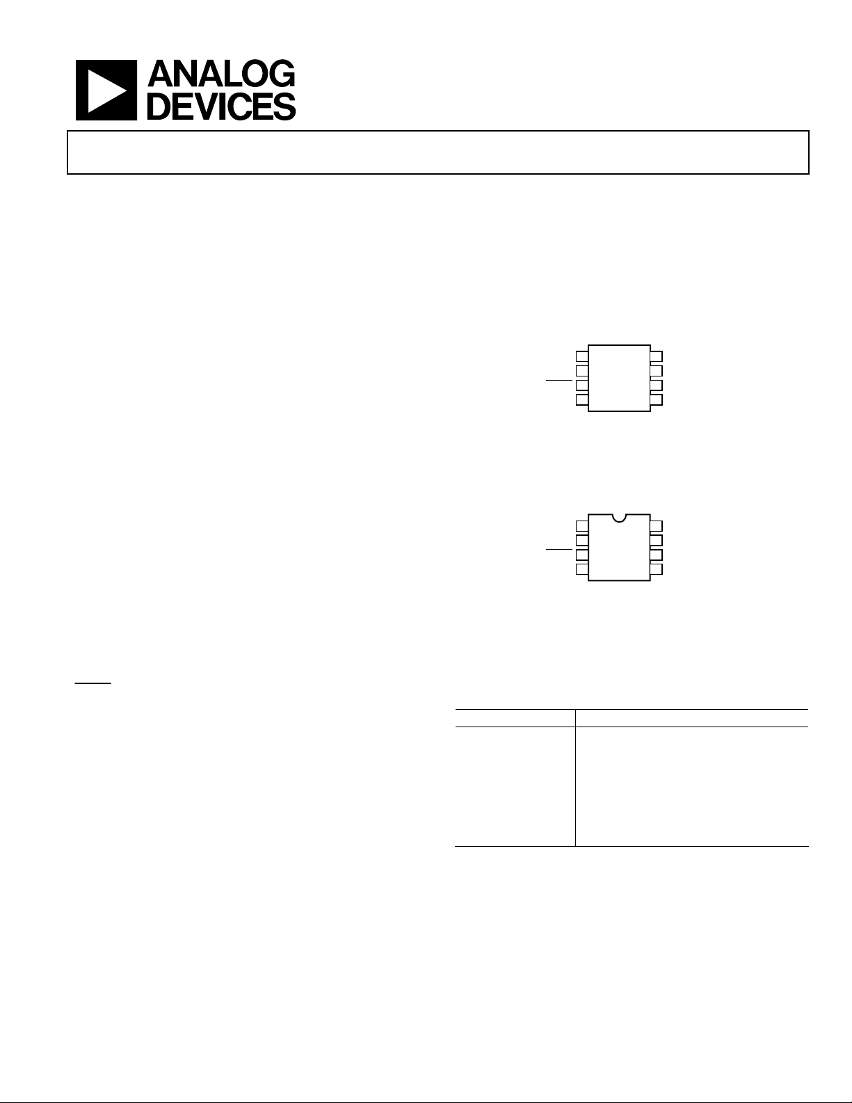
TEST PINS
Test Pin 1 and Test Pin 5 are reserved for in-package Zener zap.
To achieve the highest level of accuracy at the output, the Zener
zapping technique is used to trim the output voltage. Since each
unit may require a different amount of adjustment, the resis-
tance value at the test pins varies widely from pin to pin and
from part to part. The user should leave Pin 1 and Pin 5
unconnected.
REF19x
SERIES
TOP VIEW
(Not to Scale)
TP
1
V
S
2
SLEEP
3
GND
4
NC
NC
OUTPUT
TP
8
7
6
5
00371-001
NOTES
1. NC = NO CONNECT.
2. TP PINS ARE FACTORY TEST
POINTS, NO USER CONNECTION.
Figure 1. 8-Lead SOIC and TSSOP Pin Configuration
(S Suffix and RU Suffix)
REF19x
SERIES
TOP VIEW
(Not to Scale)
TP
1
V
S
2
SLEEP
3
GND
4
NC
NC
OUTPUT
TP
8
7
6
5
00371-002
NOTES
1. NC = NO CONNECT.
2. TP PINS ARE FACTORY TEST
POINTS, NO USER CONNECTION.
Figure 2. 8-Lead PDIP Pin Configuration
(P Suffix)
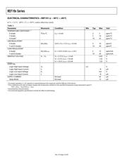
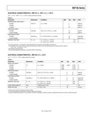
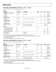
Table 1. Nominal Output Voltage
Part Number Nominal Output Voltage (V)
REF191 2.048
REF192 2.50
REF193 3.00
REF194 4.50
REF195 5.00
REF196 3.30
REF198 4.096
Verzeichnis
- ・ Konfiguration des Pinbelegungsdiagramms on Seite 1
- ・ Abmessungen des Paketumrisses on Seite 25
- ・ Teilenummerierungssystem on Seite 26
- ・ Blockdiagramm on Seite 19
- ・ Beschreibung der Funktionen on Seite 1
- ・ Technische Daten on Seite 1 Seite 3 Seite 15
- ・ Anwendungsbereich on Seite 1 Seite 19 Seite 22
- ・ Elektrische Spezifikation on Seite 3 Seite 4 Seite 5 Seite 6 Seite 7