


herunterladen

User's Guide
SLLU213–February 2015
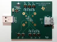
SN65LVPE512 EVM
The SN65LVPE512 is a dual-channel, single lane USB 3.0 redriver and signal conditioner that supports
data rates of 5 Gbps. This document explains how to use the LVPE512 EVM to easily evaluate the
functionality of this device in various applications.
This EVM acts as a modifiable reference design for the SN65LVPE512 that allows this device to be used
in a wide variety of applications and configurations. Table 1 explains how to modify these configuration
settings by using the switches on the EVM. Example applications for this device include notebooks,
desktops, docking stations, servers, and workstations. Schematics, printed-circuit-board (PCB) layout
images, and a bill of materials (BOM) for this module are included in this user's guide.
Contents
1 Introduction ................................................................................................................... 2
2 LVPE512 Evaluation Module............................................................................................... 2
3 Kit Contents................................................................................................................... 2
3.1 Operational Description of EVM .................................................................................. 2
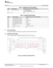
4 PCB Construction............................................................................................................ 3
4.1 EVM Board Schematics............................................................................................ 3
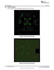
4.2 EVM PCB Layout ................................................................................................... 6
4.3 EVM PCB Fabrication.............................................................................................. 8
5 EVM Bill of Materials ........................................................................................................ 8
List of Figures
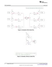
1 Schematic of High Speed Pins............................................................................................. 3
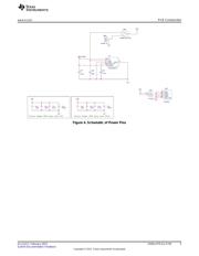
2 Schematic of EQ Control Pins ............................................................................................. 4
3 Schematic of Device Control Pins......................................................................................... 4
4 Schematic of Power Pins ................................................................................................... 5
5 PCB Layout of Top Layer................................................................................................... 6
6 PCB Layout Second Layer ................................................................................................. 6
7 PCB Layout of Third Layer ................................................................................................. 7
8 PCB Layout of Bottom Layer............................................................................................... 7
List of Tables
1 Configuration of EVM........................................................................................................ 2
2 Suggested Default Settings ................................................................................................ 3
3 SN65LVPE512 EVM Bill of Materials ..................................................................................... 8
1
SLLU213–February 2015 SN65LVPE512 EVM
Submit Documentation Feedback
Copyright © 2015, Texas Instruments Incorporated
Verzeichnis