

herunterladen

User's Guide
SLAU288A–August 2009–Revised May 2010
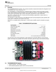
TAS5630DKD2EVM
This user’s guide describes the operation of the evaluation module for the TAS5630DKD 300W Stereo
Feedback Analog-Input Digital Amplifier from Texas Instruments. The user’s guide also provides
measurement data and design information including the schematic, BOM, and PCB layout.
Contents
1 Overview ..................................................................................................................... 3
1.1 TAS5630DKD2EVM Features .................................................................................... 3
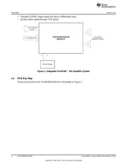
1.2 PCB Key Map ...................................................................................................... 4
2 Quick Setup Guide .......................................................................................................... 5
2.1 Electrostatic Discharge Warning ................................................................................. 5
2.2 Unpacking the EVM ................................................................................................ 5
2.3 Power Supply Setup ............................................................................................... 6
2.4 Applying Input Signal .............................................................................................. 6
2.5 Speaker Connection ............................................................................................... 6
3 Protection .................................................................................................................... 7
3.1 Short-Circuit Protection and Fault-Reporting Circuitry ........................................................ 7
3.2 Fault Reporting ..................................................................................................... 7
4 TAS5630DKD2EVM Performance ........................................................................................ 7
4.1 THD+N vs Power (BTL – 4 Ω) ................................................................................... 9
4.2 THD+N vs Power (BTL – 8 Ω) ................................................................................... 9
4.3 THD+N vs Frequency (BTL –4 Ω) .............................................................................. 10
4.4 THD+N vs Frequency (BTL –8 Ω) .............................................................................. 10
4.5 THD+N vs Power (PBTL – 2 Ω) ................................................................................ 11
4.6 THD+N vs Frequency (PBTL – 2 Ω) ........................................................................... 11
4.7 FFT Spectrum with –60-dBFS Tone (BTL) .................................................................... 11
4.8 Idle Noise FFT Spectrum (BTL) ................................................................................ 12
4.9 FFT Spectrum With –60-dBFS Tone (PBTL) ................................................................. 12
4.10 Idle Noise FFT Spectrum (PBTL) .............................................................................. 13
4.11 Channel Separation (BTL ....................................................................................... 13
4.12 Frequency Response (BTL) ..................................................................................... 14
4.13 Frequency Response (PBTL) ................................................................................... 14
4.14 High-Current Protection (BTL) .................................................................................. 15
4.15 High-Current Protection (PBTL) ................................................................................ 15
4.16 Pop/Click (BTL) ................................................................................................... 16
4.17 Pop/Click (PBTL) ................................................................................................. 16
4.18 Output Stage Efficiency .......................................................................................... 17
5 Related Documentation from Texas Instruments ..................................................................... 17
5.1 Additional Documentation ....................................................................................... 18
Appendix A Design Documents ............................................................................................... 18
List of Figures
1 Integrated PurePath™ HD Amplifier System............................................................................ 4
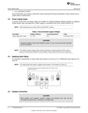
2 Physical Structure for the TAS5630PHDEVM (Approximate Layout)................................................ 5
3 THD+N vs Power (BTL – 4 Ω) ............................................................................................ 9
4 THD+N vs Power (BTL – 8 Ω) ............................................................................................ 9
PurePath is a trademark of Texas Instruments.
1
SLAU288A–August 2009–Revised May 2010 TAS5630DKD2EVM
Copyright © 2009–2010, Texas Instruments Incorporated
Verzeichnis
- ・ Blockdiagramm on Seite 18 Seite 19 Seite 20
- ・ Technische Daten on Seite 8
- ・ Anwendungsbereich on Seite 34