
herunterladen

14-Channel
Analog
Multiplexer
4.096-V and 2.048-V
Internal Reference
Sample and Hold
Input Address
Register
Reference CTRL
Output Data
Register
Internal
Oscillator
12-to-1 Data
Selector and
Driver
Control Logic and
I/O Counters
Low-Power 12-Bit
SAR ADC
V
CC
20 14 13
REF+ REF±
INT/EOC
19
16
DATA
OUT
GND
10
1
2
3
4
5
6
7
8
9
11
12
17
15
18
AIN0
AIN1
AIN2
AIN3
AIN4
AIN5
AIN6
AIN7
AIN8
AIN9
AIN10
DATA IN
I/O CLOCK
CS
4
12
12
4
3
Self Test
Product
Folder
Sample &
Buy
Technical
Documents
Tools &
Software
Support &
Community
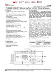
TLV2556
SLAS355B –DECEMBER 2001–REVISED DECEMBER 2015
TLV2556 12-Bit 200-kSPS 11-Channel Low-Power Serial ADC With Internal Reference
1 Features 3 Description
The TLV2556 device is a 12-bit switched-capacitor
1
• 12-Bit Resolution Analog-to-Digital Converter
successive-approximation analog-to-digital converter
(ADC)
(ADC). The ADC has three control inputs: chip select
• Up to 200-kSPS (150-kSPS for 3 V) Throughput
(CS), the input-output clock, and the address and
Over Operating Temperature Range With 12-Bit
control input (DATAIN). These inputs communicate
Output Mode
with the serial port of a host processor or peripheral
through a serial 3-state output.
• 11 Analog Input Channels
• Three Built-In Self-Test Modes
In addition to the high-speed converter and versatile
control capability, the device has an on-chip 14-
• Inherent Sample and Hold Function
channel multiplexer that can select any one of 11
• Programmable Reference Source (2.048 / 4.096 V
inputs or any one of three internal self-test voltages
Internal or External)
using configuration register 1. The sample-and-hold
• Inherent Sample and Hold Function
function is automatic. At the end of conversion, when
programmed as EOC, the pin 19 output goes high to
• Linearity Error of ±1 LSB (Maximum)
indicate that conversion is complete. If pin 19 is
• On-Chip Conversion Clock
programmed as INT, the signal goes low when the
• Programmable Conversion Status Output: INT or
conversion is complete. The converter incorporated in
EOC
the device features differential, high-impedance
reference inputs that facilitate ratiometric conversion,
• Unipolar or Bipolar Output Operation
scaling, and isolation of analog circuitry from logic
• Programmable Most Significant Bit (MSB) or Least
and supply noise. A switched-capacitor design allows
Significant Bit (LSB) First
low error conversion over the full operating
• Programmable Power Down
temperature range. An internal reference is available
and its voltage level is programmable through
• Programmable Output Data Length
configuration register 2 (CFGR2).
• SPI-Compatible Serial Interface With I/O Clock
Frequencies Up to 15 MHz (CPOL = 0,
The TLV2556 is characterized for operation from
CPHA = 0) T
A
= –40°C to +85°C.
Device Information
(1)
2 Applications
PART NUMBER PACKAGE BODY SIZE (NOM)
• Industrial Process Control
SOIC (20) 7.50 mm × 12.80 mm
• Portable Data Logging
TLV2556
TSSOP (20) 4.40 mm × 6.50 mm
• Battery-Powered Instruments
(1) For all available packages, see the package option addendum
• Automotive
at the end of the data sheet.
Block Diagram
1
An IMPORTANT NOTICE at the end of this data sheet addresses availability, warranty, changes, use in safety-critical applications,
intellectual property matters and other important disclaimers. PRODUCTION DATA.
Verzeichnis
- ・ Konfiguration des Pinbelegungsdiagramms on Seite 3
- ・ Abmessungen des Paketumrisses on Seite 35 Seite 37 Seite 38
- ・ Markierungsinformationen on Seite 35 Seite 36
- ・ Blockdiagramm on Seite 1 Seite 22 Seite 30 Seite 33
- ・ Typisches Anwendungsschaltbild on Seite 30 Seite 31
- ・ Technische Daten on Seite 4 Seite 6
- ・ Anwendungsbereich on Seite 1 Seite 36 Seite 39
- ・ Elektrische Spezifikation on Seite 5 Seite 6