
herunterladen
TMS320C5504
www.ti.com
SPRS659G –AUGUST 2010–REVISED SEPTEMBER 2013
TMS320C5504 Fixed-Point Digital Signal Processor
Check for Samples: TMS320C5504
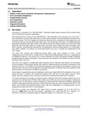
1 Fixed-Point Digital Signal Processor
1.1 Features
12
• High-Performance, Low-Power, TMS320C55x™ • Master/Slave Inter-Integrated Circuit (I
2
C Bus™)
Fixed-Point Digital Signal Processor
• Four Inter-IC Sound (I
2
S Bus™) for Data
– 16.67-, 13.33-, 10-, 8.33-, 6.66-ns Instruction Transport
Cycle Time
• Device USB Port With Integrated 2.0 High-
– 60-, 75-, 100-, 120-, 150-MHz Clock Rate Speed PHY that Supports:
– One/Two Instructions Executed per Cycle – USB 2.0 Full- and High-Speed Device
– Dual Multipliers [Up to 200, 240, or 300 • Real-Time Clock (RTC) With Crystal Input, With
Million Multiply-Accumulates per Second Separate Clock Domain and Power Supply
(MMACS)]
• Four Core Isolated Power Supply Domains:
– Two Arithmetic/Logic Units (ALUs) Analog, RTC, CPU and Peripherals, and USB
– Three Internal Data/Operand Read Buses • Four I/O Isolated Power Supply Domains: RTC
and Two Internal Data/Operand Write Buses I/O, EMIF I/O, USB PHY, and DV
DDIO
– Software-Compatible With C55x Devices • One integrated LDO (ANA_LDO) to power DSP
PLL (V
DDA_PLL
)
– Industrial Temperature Devices Available
• Low-Power S/W Programmable Phase-Locked
• 256K Bytes Zero-Wait State On-Chip RAM,
Loop (PLL) Clock Generator
Composed of:
• On-Chip ROM Bootloader (RBL) to Boot From
– 64K Bytes of Dual-Access RAM (DARAM),
NAND Flash, NOR Flash, SPI EEPROM, SPI
8 Blocks of 4K x 16-Bit
Serial Flash or I2C EEPROM
– 192K Bytes of Single-Access RAM (SARAM),
• IEEE-1149.1 (JTAG)
24 Blocks of 4K x 16-Bit
Boundary-Scan-Compatible
• 128K Bytes of Zero Wait-State On-Chip ROM
• Up to 26 General-Purpose I/O (GPIO) Pins
(4 Blocks of 16K x 16-Bit)
(Multiplexed With Other Device Functions)
• 4M x 16-Bit Maximum Addressable External
• 196-Terminal Pb-Free Plastic BGA (Ball Grid
Memory Space (SDRAM/mSDRAM)
Array) (ZCH Suffix)
• 16-/8-Bit External Memory Interface (EMIF) with
• 1.05-V Core (60 or 75 MHz), 1.8-V, 2.5-V, 2.75-V,
Glueless Interface to:
or 3.3-V I/Os
– 8-/16-Bit NAND Flash, 1- and 4-Bit ECC
• 1.3-V Core (100, 120 MHz), 1.8-V, 2.5-V, 2.75-V,
– 8-/16-Bit NOR Flash
or 3.3-V I/Os
– Asynchronous Static RAM (SRAM)
• 1.4-V Core (150 MHz), 1.8-V, 2.5-V, 2.75-V or 3.3-
– 16-bit SDRAM/mSDRAM (1.8-, 2.5-, 2.75-, and
V I/Os
3.3-V)
• Direct Memory Access (DMA) Controller
– Four DMA With 4 Channels Each (16-
Channels Total)
• Three 32-Bit General-Purpose Timers
– One Selectable as a Watchdog and/or GP
• Two MultiMedia Card/Secure Digital (MMC/SD)
Interfaces
• Universal Asynchronous Receiver/Transmitter
(UART)
• Serial-Port Interface (SPI) With Four Chip-
Selects
1
Please be aware that an important notice concerning availability, standard warranty, and use in critical applications of
Texas Instruments semiconductor products and disclaimers thereto appears at the end of this data sheet.
2All trademarks are the property of their respective owners.
PRODUCTION DATA information is current as of publication date. Products conform to
Copyright © 2010–2013, Texas Instruments Incorporated
specifications per the terms of the Texas Instruments standard warranty. Production
processing does not necessarily include testing of all parameters.
Verzeichnis
- ・ Konfiguration des Pinbelegungsdiagramms on Seite 15 Seite 52 Seite 55
- ・ Abmessungen des Paketumrisses on Seite 140
- ・ Markierungsinformationen on Seite 140
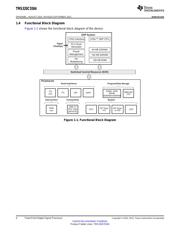
- ・ Blockdiagramm on Seite 4
- ・ Typisches Anwendungsschaltbild on Seite 119
- ・ Beschreibung der Funktionen on Seite 52
- ・ Technische Daten on Seite 12 Seite 61 Seite 66 Seite 67 Seite 68
- ・ Anwendungsbereich on Seite 2 Seite 143
- ・ Elektrische Spezifikation on Seite 12 Seite 39 Seite 59 Seite 63 Seite 64