

herunterladen

User's Guide
SLVU433–February 2011
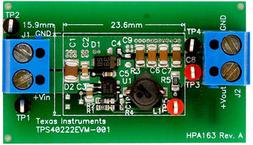
TPS53128EVM-620
The TPS53128EVM-620 Evaluation Module presents an easy-to-use reference design for a common dual
output power supply using the TPS53128 controller in cost sensitive applications.
Contents
1 Introduction .................................................................................................................. 2
1.1 Description .......................................................................................................... 2
1.2 Application .......................................................................................................... 2
1.3 Features ............................................................................................................. 2
2 Electrical Performance Specifications .................................................................................... 2
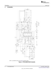
3 Schematics ................................................................................................................... 4
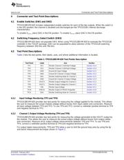
4 Connector and Test Point Descriptions .................................................................................. 5
4.1 Enable Switches (SW1 and SW2) ............................................................................... 5
4.2 Switching Frequency Select Switch (SW3) ..................................................................... 5
4.3 Test Point Descriptions ............................................................................................ 5
5 Test Setup ................................................................................................................... 7
5.1 Equipment ........................................................................................................... 7
5.2 Recommended Setup ............................................................................................. 7
6 Test Procedure .............................................................................................................. 9
6.1 Start-up Procedure ................................................................................................. 9
6.2 Line/Load Regulation and Efficiency Measurement Procedure .............................................. 9
6.3 Output Ripple Voltage Measurement Procedure .............................................................. 9
6.4 Shutdown Procedure .............................................................................................. 9
7 Performance Data and Typical Characteristic Curves ................................................................. 9
7.1 Efficiency .......................................................................................................... 10
7.2 Line and Load Regulation ....................................................................................... 10
7.3 Output Voltage Ripple ........................................................................................... 11
7.4 Switch Node Waveforms ........................................................................................ 11
8 EVM Assembly Drawings and Layout .................................................................................. 11
9 Bill of Materials ............................................................................................................. 15
List of Figures
1 TPS53128EVM-620 Schematic. .......................................................................................... 4
2 Tip and Barrel Measurement for Output Voltage Ripple............................................................... 6
3 TPS53128EVM-620 Recommended Test Setup ....................................................................... 8
4 Efficiency vs Load ........................................................................................................ 10
5 Efficiency vs Load ........................................................................................................ 10
6 Output Voltage vs Load .................................................................................................. 10
7 Output Voltage vs Load .................................................................................................. 10
8 Output Voltage Ripple .................................................................................................... 11
9 Output Voltage Ripple .................................................................................................... 11
10 Switching Waveform ...................................................................................................... 11
11 Switching Waveform ...................................................................................................... 11
12 Top Assembly.............................................................................................................. 12
13 Bottom Assembly.......................................................................................................... 12
1
SLVU433–February 2011 TPS53128EVM-620
Submit Documentation Feedback
© 2011, Texas Instruments Incorporated
Verzeichnis
- ・ Blockdiagramm on Seite 4 Seite 15
- ・ Technische Daten on Seite 3
- ・ Anwendungsbereich on Seite 17
- ・ Elektrische Spezifikation on Seite 9 Seite 10