
herunterladen

User's Guide
SLVU478– June 2011
TPS6126x, Low-Input Voltage, Boost Converter Evaluation
Module
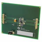
This user’s guide describes the TPS6126x evaluation module (EVM) and how to perform a stand-alone
evaluation to allow the EVM to interface with the system and host. The TPS61260EVM-673 converter is
programmed from the factory to deliver a 3.3-Vdc output voltage for a continuous load of up to 100 mA.
The boost converter can be enabled or disabled with the JP1 shunt jumper. Other options with a fixed
output voltage are available.
Contents
1 Introduction .................................................................................................................. 2
2 Considerations When Evaluating the TPS6126x ....................................................................... 2
3 Performance Specification Summary ..................................................................................... 2
4 Test Summary ............................................................................................................... 2
4.1 Equipment ........................................................................................................... 3
4.2 Equipment and EVM Setup ....................................................................................... 3
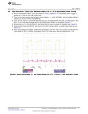
4.3 Test Procedure – Input: One Alkaline Battery Cell (1.5 V) or Equivalent Power Source ................. 5
5 Schematic, Physical Layouts, and Bill of Materials ..................................................................... 7
5.1 Schematic ........................................................................................................... 7
5.2 Physical Layouts ................................................................................................... 8
5.3 Bill of Materials .................................................................................................... 11
List of Figures
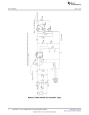
1 EVM Schematic and Evaluation Setup................................................................................... 4
2 Boost Switch Node, V_L and Output Ripple; Vin = 1.5 V, Vout = 3.3 Vdc With 49.9-Ω Load.................... 5
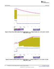
3 Power Down With Enable: Boost Switch Node, V_L, Output, Enable; Vin = 1.5 V, Vout = 3.3 Vdc With
49.9-Ω Load ................................................................................................................. 6
4 Power-Up With Enable: Boost Switch Node, V_L, Output, Enable; Vin = 1.5 V, Vout = 3.3 Vdc With
49.9-Ω Load ................................................................................................................. 6
5 Schematic.................................................................................................................... 7
6 Assembly Layer ............................................................................................................. 8
7 Top Layer .................................................................................................................... 9
8 Bottom Layer............................................................................................................... 10
List of Tables
1 Setup I/O Connections and Configuration for Evaluation of TPS61260EVM ....................................... 3
2 HPA673A Bill of Materials................................................................................................ 11
PowerPAD is a trademark of Texas Instruments.
1
SLVU478–June 2011 TPS6126x, Low-Input Voltage, Boost Converter Evaluation Module
Submit Documentation Feedback
Copyright © 2011, Texas Instruments Incorporated
Verzeichnis