
herunterladen
User's Guide
SLVU405–August 2010
TPS7A30-49EVM-567
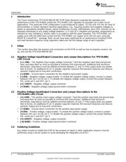
This user’s guide describes the characteristics, operation, and use of theTPS7A30-49EVM-567 Evaluation
Module (EVM) as a reference design to facilitate engineering evaluation of the TPS7A3001 negative
voltage low-dropout (LDO) regulator and/or the TPS7A4901 positive voltage LDO regulator for individual
or split-rail applications. Included in this user’s guide are setup instructions, a schematic diagram, layout
and thermal guidelines, a bill of materials, and test results.
Contents
1 Introduction .................................................................................................................. 2
2 Setup ......................................................................................................................... 2
2.1 Negative Voltage Input/Output Connectors and Jumper Descriptions For TPS7A3001 LDO Circuit
........................................................................................................................ 2
2.2 Positive Voltage Input/Output Connectors and Jumper Descriptions fo the TPS7A4901 LDO
Circuit ................................................................................................................ 2
2.3 Soldering Guidelines ............................................................................................... 2
2.4 Equipment Interconnect ........................................................................................... 3
3 Operation ..................................................................................................................... 3
4 Adjustable Operation ....................................................................................................... 3
5 Test Results ................................................................................................................. 4
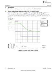
5.1 Turnon Output Ramp: Negative Voltage LDO, TPS7A3001 Circuit ......................................... 4
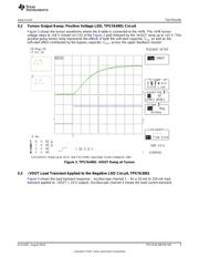
5.2 Turnon Output Ramp: Positive Voltage LDO, TPS7A4901 Circuit .......................................... 5
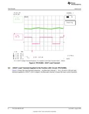
5.3 –VOUT Load Transient Applied to the Negative LDO Circuit, TPS7A3001 ................................ 5
5.4 +VOUT Load Transient Applied to the Positive LDO Circuit, TPS7A4901. ................................ 6
6 Thermal Guidelines ......................................................................................................... 7
7 Board Layout ................................................................................................................ 8
8 Schematic and Bill of Materials .......................................................................................... 11
8.1 Schematic ......................................................................................................... 11
8.2 Bill of Materials .................................................................................................... 12
List of Figures
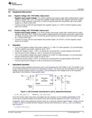
1 LDO Schematic Showing the R
1
and R
2
Adjustment Resistors....................................................... 3
2 TPS7A3001 –VOUT Ramp at Turnon.................................................................................... 4
3 TPS7A4901 +VOUT Ramp at Turnon.................................................................................... 5
4 TPS7A3001 –VOUT Load Transient ..................................................................................... 6
5 TPS7A4901 +VOUT Load Transient ..................................................................................... 7
6 Assembly Layer ............................................................................................................. 8
7 Top Layer Routing .......................................................................................................... 9
8 Bottom Layer Routing..................................................................................................... 10
9 TPS7A30-49EVM-567 Schematic....................................................................................... 11
List of Tables
1 Thermal Resistance, q
JA
, and Maximum Power Dissipation........................................................... 8
2 TPS7A30-49EVM-567 Bill of Materials ................................................................................. 12
PowerPAD is a trademark of Texas Instruments.
1
SLVU405–August 2010 TPS7A30-49EVM-567
Copyright © 2010, Texas Instruments Incorporated
Verzeichnis
- ・ Blockdiagramm on Seite 3 Seite 11 Seite 12
- ・ Schweißen Temperatur on Seite 2
- ・ Anwendungsbereich on Seite 14
- ・ Elektrische Spezifikation on Seite 3
- ・ Teilenummernliste on Seite 7