
herunterladen
Pinout
KE02 Sub-Family Data Sheet, Rev. 5, 07/2016
NXP Semiconductors
31
KE02 Sub-Family Data Sheet, Rev. 5, 07/2016
31
NXP Semiconductors
NXP Semiconductors
Document Number MKE02P64M20SF0
Data Sheet: Technical Data
Rev. 5, 07/2016
MKE02P64M20SF0
KE02 Sub-Family Data Sheet
Supports the following: MKE02Z16VLC2(R), MKE02Z32VLC2(R),
MKE02Z64VLC2(R), MKE02Z16VLD2(R), MKE02Z32VLD2(R),
MKE02Z64VLD2(R), MKE02Z32VLH2(R), MKE02Z64VLH2(R),
MKE02Z32VQH2(R), and MKE02Z64VQH2(R)
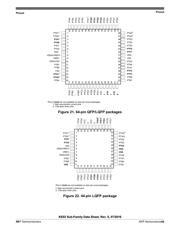
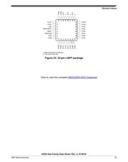
Pinout
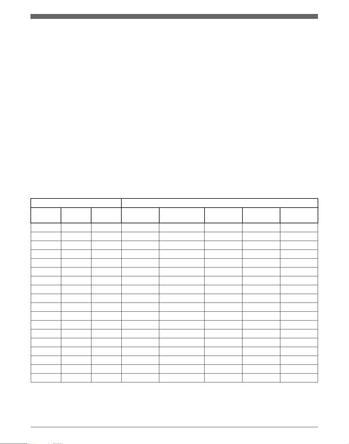
Signal multiplexing and pin assignments
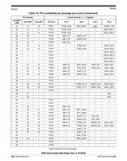
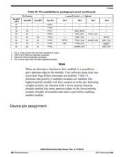
The following table shows the signals available on each pin and the locations of these
pins on the devices supported by this document. The Port Control Module is responsible
for selecting which ALT functionality is available on each pin.
Table 19. Pin availability by package pin-count
Pin Number Lowest Priority < ---- > Highest
64-QFP/
LQFP
44-LQFP 32-LQFP Port Pin Alt 1 Alt 2 Alt 3 Alt 4
1
1
1
PTD1
1
KBI1_P1 FTM2_CH3 SPI1_MOSI —
2
2
2
PTD0
1
KBI1_P0
FTM2_CH2
SPI1_SCK
—
3
— — PTH7 — — — —
4
—
—
PTH6
—
—
—
—
5
3
— PTE7 — FTM2_CLK — FTM1_CH1
6
4
—
PTH2
—
BUSOUT
—
FTM1_CH0
7
5
3
— — — — VDD
8
6
4
—
—
—
VDDA
VREFH
2
9
7
5
— — — — VREFL
10
8
6
—
—
—
VSSA
VSS
3
11
9
7
PTB7 — I2C0_SCL — EXTAL
12
10
8
PTB6
—
I2C0_SDA
—
XTAL
13
11 — — — — — VSS
14
—
—
PTH1
1
—
FTM2_CH1
—
—
15
— — PTH0
1
— FTM2_CH0 — —
16
—
—
PTE6
—
—
—
—
17
— — PTE5 — — — —
18
12
9
PTB5
1
FTM2_CH5
SPI0_PCS0
ACMP1_OUT
—
Table continues on the next page...
Verzeichnis