AN-1225
APPLICATION NOTE
One Technology Way • P. O. Box 9106 • Norwood, MA 02062-9106, U.S.A. • Tel: 781.329.4700 • Fax: 781.461.3113 • www.analog.com
32 Channels of Programmable Voltage with Excellent Temperature Drift
Performance Using the AD5382 DAC
Rev. B | Page 1 of 2
CIRCUIT FUNCTION AND BENEFITS
This circuit is a multichannel digital-to-analog converter (DAC)
configuration with excellent temperature drift performance. It
provides 32 individual voltage channels with 14 bits of resolution
and a temperature stability of typically less than 3 ppm/°C.
CIRCUIT DESCRIPTION
Table 1. Devices Connected/Referenced
Product Description
AD5382 32-channel 14-bit 3 V/5 V single-supply DAC
ADR421 Low noise, 2.500 V XFET® voltage reference
ADR431 Ultralow noise XFET voltage reference
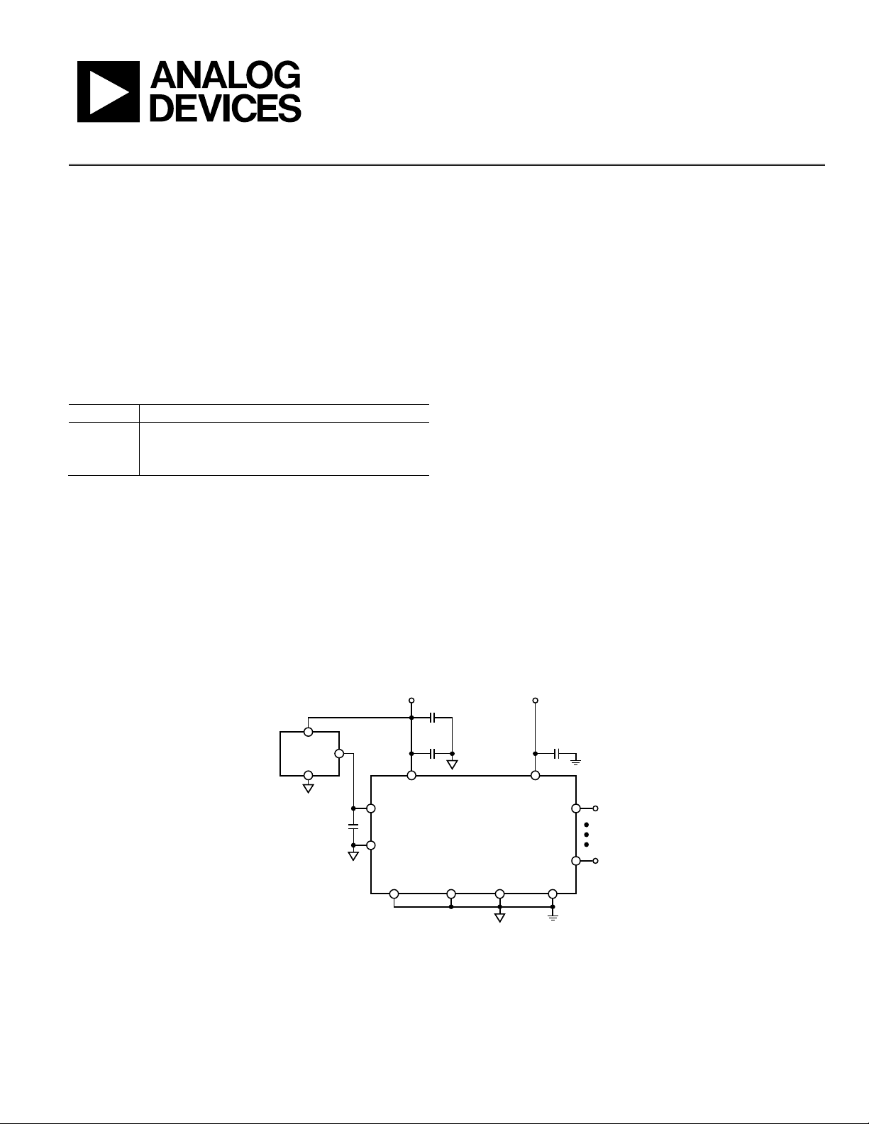
Figure 1 shows a typical configuration for the AD5382 when
configured for use with an external reference. In the circuit
shown, all AGND, SIGNAL_GND, and DAC_GND pins are
tied together to a common AGND. AGND and DGND are
connected together at the
AD5382 device. On power-up, the
AD5382 defaults to external reference operation.
This design uses two separate 5.0 V power supplies: one to power
the voltage reference and the analog portion of the
AD5382
(AVDD), and the other to power the digital portion of the
AD5382 (DVDD). For best performance, always use a linear
regulator to power the analog portion of the circuit. If a switching
regulator is used to power the digital portion, take care to minimize
switching noise at the DVDD supply pins. Additional decoupling
using a series connected ferrite bead may be required. The
AD5382 digital (DVDD) power supply can operate from a 3 V
or 5 V supply, which provides for maximum flexibility when
interfacing to digital components. Both supplies can be tied
together to a common 5 V supply, provided that supply is
derived from a linear regulator. Refer to the ADIsimPower
design tool for guidance on the power supply designs.
It is recommended to decouple close to the device with a 0.1 µF
ceramic and a 10 µF tantalum capacitor. In this circuit, the
reference for the
AD5382 is provided externally from either an
ADR421 or ADR431 2.5 V reference. The ADR431 provides a
lower output voltage noise specification for applications where
that specification is important. Decouple the reference at the
REFOUT/REFIN pin of the device with a 0.1 µF capacitor.
COMMON VARIATIONS
A variation of this circuit is the AD5382-3 with the ADR280 1.2 V
reference where all other connections and components are the
same as those previously outlined.
08203-001
ADR431/
ADR421
AD5382-5
AVDD DVDD
SIGNAL_GNDDAC_GND DGND
VOUT31
VOUT0
AGND
REFOUT/REFIN
REFGND
0.1µF
10µF 0.1µF
0.1µF
5.0V
2.5V
5.0V
Figure 1. AD5382 Typical Configuration with External Reference (Simplified Schematic)


