

herunterladen
Cascadable IF VGAs with
Programmable RMS Detectors
Data Sheet
ADL5336
Rev. B
Information furnished by Analog Devices is believed to be accurate and reliable. However, no
responsibility is assumed by Analog Devices for its use, nor for any infringements of patents or other
rights of third parties that may result from its use. Specifications subject to change without notice. No
license is granted by implication or otherwise under any patent or patent rights of Analog Devices.
Trademarks and registered trademarks are the property of their respective owners.
One Technology Way, P.O. Box 9106, Norwood, MA 02062-9106, U.S.A.
Tel: 781.329.4700 www.analog.com
Fax: 781.461.3113 ©2011–2012 Analog Devices, Inc. All rights reserved.
FEATURES
Pair of VGAs with rms AGC detectors
VGA and AGC modes of operation
Continuous gain control range: 48 dB
Noise figure (NF) = 6.8 dB at maximum gain
IMD3 > 62 dBc for 1.0 V p-p composite output
Differential input and output
Multiplexed inputs for VGA2
Programmable detector AGC setpoints
Programmable VGA maximum gain
Power-down feature
Single 5 V supply operation
APPLICATIONS
Point-to-multipoint radios
Instrumentation
Medical
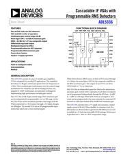
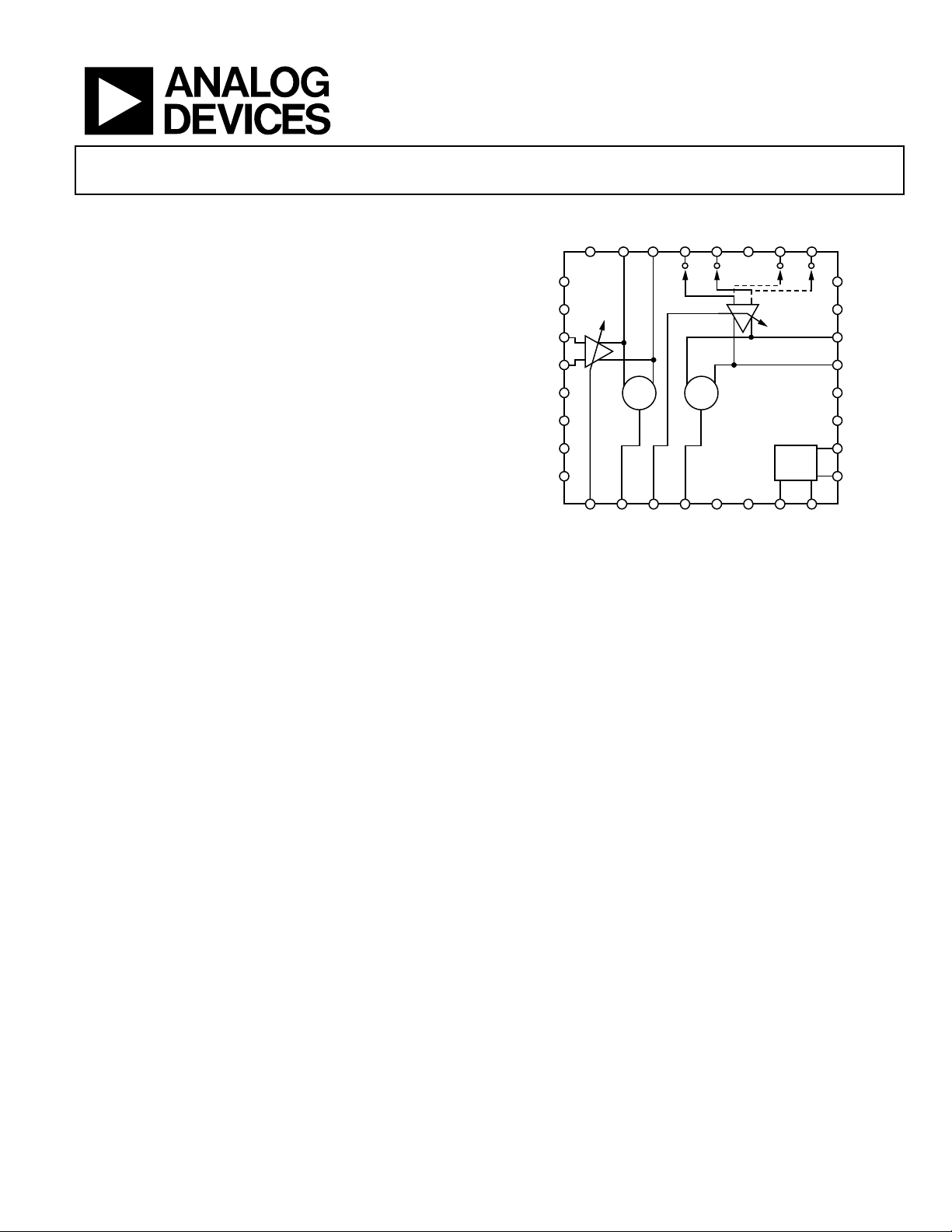
FUNCTIONAL BLOCK DIAGRAM
Figure 1.
GENERAL DESCRIPTION
The ADL5336 consists of a pair of variable gain amplifiers
(VGAs) designed for cascaded IF applications. The amplifiers
have linear-in-dB gain control and operate from low frequencies to
1 GHz. Their excellent gain conformance over the control range
and flatness over frequency are due to Analog Devices, Inc.,
patented X-AMP® architecture, an innovative technique for
implementing high performance variable gain control.
Each VGA has 24 dB of gain control range. Their maximum gain
can be independently programmable over a 6 dB range via the
SPI. The VGAs can be cascaded to provide a total range of 48 dB.
When connected to a 50 source through a 1:4 balun, the gain
is 6 dB higher. The second VGA has an SPI programmable input
switch that selects one of two external inputs.
When driven from a 200 Ω source or from a 50 Ω source through
a 1:4 balun, the noise figure (NF) for the composite amplifier is
6.8 dB at maximum gain. The output of each VGA can drive
100 Ω loads to 5 V p-p maximum.
Each VGA has an independent square law detector for autonomous,
automatic gain control (AGC) operation. Each detector setpoint
can be programmed independently through the SPI from −24 dBV
to −3 dBV in 3 dB steps. When both VGAs are arranged in AGC
mode and are programmed to the same setpoint, the composite NF
increases to 9 dB when backed off by 18 dB from maximum gain.
The ADL5336 operates from a 5 V supply and consumes a typical
supply current of 80 mA. When disabled, it consumes 4 mA. It is
fabricated in an advanced silicon-germanium BiCMOS process and
is available in a 32-lead exposed paddle LFCSP package. Performance
is specified over a −40°C to +85°C temperature range.
ADL5336
09550-001
VCM1
VPOS
VPOS
COM
MODE
ENBL
INP1
INM1
VPOS
VPOS
COM
SDO
DATA
OPP2
VCM2
COM
OPM2
OPP1 OPM1 IP2
A
IM2
A
COM IP2B IM2B
GAIN1 DTO1 GAIN2 DTO2 COMD VPSD LE CLK
X
2
X
2
SPI
VGA1
VGA2
Verzeichnis
- ・ Konfiguration des Pinbelegungsdiagramms on Seite 8 Seite 31
- ・ Abmessungen des Paketumrisses on Seite 31
- ・ Teilenummerierungssystem on Seite 31
- ・ Blockdiagramm on Seite 1 Seite 18 Seite 21 Seite 26 Seite 27
- ・ Beschreibung der Funktionen on Seite 1 Seite 8 Seite 31
- ・ Technische Daten on Seite 1 Seite 4 Seite 7
- ・ Anwendungsbereich on Seite 1 Seite 21
- ・ Elektrische Spezifikation on Seite 9