

herunterladen
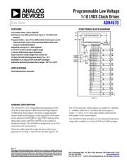
Programmable Low Voltage
1:10 LVDS Clock Driver
Data Sheet
ADN4670
Rev. A
Information furnished by Analog Devices is believed to be accurate and reliable. However, no
responsibility is assumed by Analog Devices for its use, nor for any infringements of patents or other
rights of third parties that may result from its use. Specifications subject to change without notice. No
license is granted by implication or otherwise under any patent or patent rights of Analog Devices.
Trademarks and registered trademarks are the property of their respective owners.
One Technology Way, P.O. Box 9106, Norwood, MA 02062-9106, U.S.A.
Tel: 781.329.4700
www.analog.com
Fax: 781.461.3113 ©2010–2012 A
nalog Devices, Inc. All rights reserved.
FEATURES
Low output skew <30 ps (typical)
Distributes one differential clock input to 10 LVDS clock
outputs
Programmable—one of two differential clock inputs can be
selected (CLK0, CLK1) and individual differential clock
outputs enabled/disabled
Signaling rate up to 1.1 GHz (typical)
2.375 V to 2.625 V power supply range
±100 mV differential input threshold
Input common-mode range from rail-to-rail
I/O pins fail-safe during power-down: V
DD
= 0 V
Available in 32-lead LFCSP and LQFP packages
Industrial operating temperature range: −40°C to +85°C
APPLICATIONS
Clock distribution networks
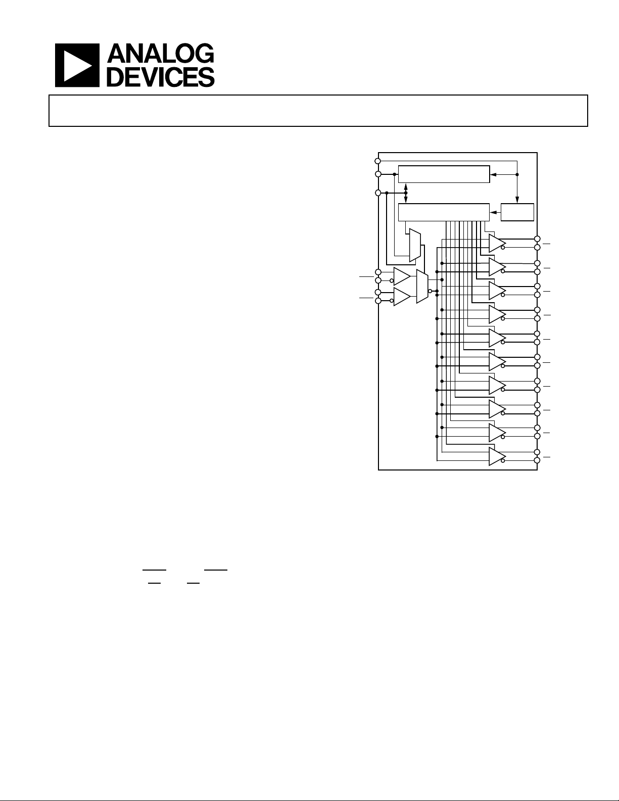
FUNCTIONAL BLOCK DIAGRAM
9876543210
10
12-BIT
COUNTER
11-BIT SHIFT REGISTER
11-BIT CONTROL REGISTER
Q9
Q8
Q7
Q6
Q5
Q4
Q3
Q2
Q1
Q0
CK
SI
EN
CLK0
CLK1
MUX
MUX
1
0
CLK0
CLK1
Q9
Q8
Q7
Q6
Q5
Q4
Q3
Q2
Q1
Q0
0
1
08870-001
Figure 1.
GENERAL DESCRIPTION
The ADN4670 is a low voltage differential signaling (LVDS)
clock driver that expands a differential clock input signal to
10 differential clock outputs. The device is programmable
using a simple serial interface, so that one of two clock inputs
can be selected (CLK0/
CLK0
or CLK1/
CLK1
) and any of the
differential outputs (Q0/
Q0
to Q9/
Q9
) can be enabled or
disabled (tristated). The ADN4670 is designed for use in 50 Ω
transmission line environments.
When the enable input EN is high, the device may be pro-
grammed by clocking 11 data bits into the shift register. The
first 10 bits determine which outputs are enabled (0 = disabled,
1 = enabled), while the 11
th
bit selects the clock input (0 =
CLK0, 1 = CLK1). A 12
th
clock pulse transfers data from the
shift register to the control register.
The ADN4670 is fully specified over the industrial temperature
range and is available in a 32-lead LFCSP and LQFP packages.
Verzeichnis
- ・ Konfiguration des Pinbelegungsdiagramms on Seite 8 Seite 10
- ・ Abmessungen des Paketumrisses on Seite 10
- ・ Teilenummerierungssystem on Seite 10
- ・ Blockdiagramm on Seite 1
- ・ Schweißen Temperatur on Seite 7
- ・ Beschreibung der Funktionen on Seite 1 Seite 8 Seite 10
- ・ Technische Daten on Seite 1 Seite 4 Seite 7
- ・ Anwendungsbereich on Seite 1