

herunterladen
Tiny I2C Programmable Linear Battery Charger with
Power Path and USB Mode Compatibility
Preliminary Technical Data
ADP5061
Rev. PrA
Information furnished by Analog Devices is believed to be accurate and reliable. However, no
responsibility is assumed by Analog Devices for its use, nor for any infringements of patents or other
rights of third parties that may result from its use. Specifications subject to change without notice. No
license is granted by implication or otherwise under any patent or patent rights of Analog Devices.
Trademarks and register ed tr ademarks ar e the prop erty of their respective owner s.
One Technology Way, P.O. Box 9106, Norwood, MA 02062-9106, U.S.A.
Tel: 781.329.47
www.analog.com
'BYª"OBMPH%FWJDFT*OD"MMSJHIUTSFTFSWFE
FEATURES
2.6mm x 2mm WLCSP Package
Fully programmable via I
2
C
Flexible digital control inputs
Up to 2.1A current from an AC charger while in LDO mode
Operating input voltage from 4.0V up to 7.0V
Tolerant input voltage -0.5V to 20V (USB VBUS)
Fully compatible with USB 3.0 and USB battery charging
specification 1.2
Built-in current sensing and limiting
Down to 32 mΩ battery isolation FET between battery and
charger output
Thermal regulation prevents over heating
Compliant with JEITA 1 and JEITA 2 Li-Ion battery charging
temperature specifications
SYS_EN flag permits the system to be disabled until battery
is at minimum required level for guaranteed system start-
up.
APPLICATIONS
Digital Still Cameras
Digital Video Cameras
Single Cell Li-Ion Portable Equipment
PDA’s, Audio, GPS Devices
Portable Medical Devices
Mobile Phones
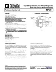
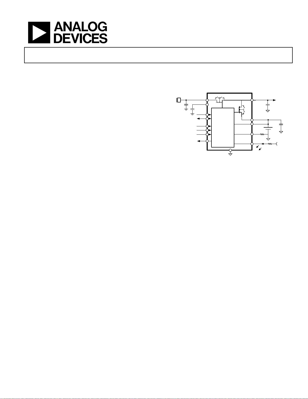
FUNCTIONAL BLOCK DIAGRAM
VIN
VBUS
AC OR
USB
SCL
SDA
DIG_IO1
DIG_IO2
DIG_IO3
AGND
+
Li-ion
THR
ISO_B
ISO_S
BAT_SNS
ADP5061
SYS_EN
System
PROGRAMMABLE
ILED
VLED
CBP
CHARGER
CONTROL
BLOCK
GENERAL DESCRIPTION
The ADP5061 charger is fully compliant with the USB 3.0 and
USB Battery Charging Specification 1.2 and enables charging
via the mini USB VBUS pin from a wall charger, car charger, or
USB Host port.
The ADP5061 operates from a 4V to 7.0V input voltage range
but is tolerant of voltages up to 20V. This alleviates the
concerns about the USB bus spiking during disconnect or
connect scenarios.
The ADP5061 also features an internal FET between the linear
charger output and the battery. This permits battery isolation
and hence system powering under a dead battery or no battery
scenario, which allows for immediate system function on
connection to a USB power supply.
Based on the type of USB source, which is detected by an
external USB detection chip, the ADP5061 can be set to apply
the correct current limit for optimal charging and USB
compliance.
The ADP5061 has 3 fuse programmable digital input/output
pins providing maximum flexibility for different systems. These
programmable digital output / input pins permit combinations
of features such as, input current limits, charging enable-
disable, charging current limits and dedicated interrupt output
pin.
Figure 1.
Verzeichnis
- ・ Konfiguration des Pinbelegungsdiagramms on Seite 8 Seite 12
- ・ Abmessungen des Paketumrisses on Seite 39
- ・ Teilenummerierungssystem on Seite 39
- ・ Blockdiagramm on Seite 1 Seite 14
- ・ Schweißen Temperatur on Seite 7
- ・ Beschreibung der Funktionen on Seite 1 Seite 8
- ・ Technische Daten on Seite 1 Seite 3 Seite 4 Seite 5 Seite 6
- ・ Anwendungsbereich on Seite 1 Seite 32
- ・ Elektrische Spezifikation on Seite 9