
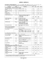
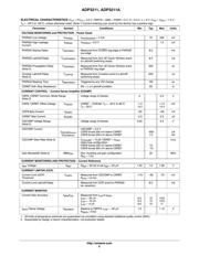
herunterladen
© Semiconductor Components Industries, LLC, 2009
November, 2009 − Rev. 2
1 Publication Order Number:
ADP3211/D
ADP3211, ADP3211A
7-Bit, Programmable,
Single-Phase, Synchronous
Buck Controller
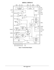
The ADP3211 is a highly efficient, single−phase, synchronous
buck switching regulator controller. With its integrated driver, the
ADP3211 is optimized for converting the notebook battery voltage to
the supply voltage required by high performance Intel chipsets. An
internal 7−bit DAC is used to read a VID code directly from the
chip−set or the CPU and to set the GMCH render voltage or the CPU
core voltage to a value within the range of 0 V to 1.5 V.
The ADP3211 uses a multi−mode architecture. It provides
programmable switching frequency that can be optimized for
efficiency depending on the output current requirement. In addition,
the ADP3211 includes a programmable load line slope function to
adjust the output voltage as a function of the load current so that the
core voltage is always optimally positioned for a load transient. The
ADP3211 also provides accurate and reliable current overload
protection and a delayed power−good output. The IC supports
On−The−Fly (OTF) output voltage changes requested by the chip−set.
The ADP3211 has a boot voltage of 1.1 V for IMVP−6.5
applications in CPU mode. The ADP3211A has a boot voltage of
1.2 V in CPU mode.
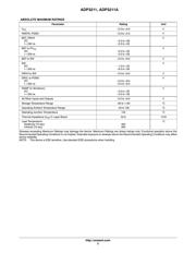
The ADP3211 is specified over the extended commercial temperature
range of −40°C to 100°C and is available in a 32−lead QFN.
Features
• Single−Chip Solution
♦ Fully Compatible with the Intel
®
IMVP−6.5t CPU and GMCH
Chipset Voltage Regulator Specifications Integrated MOSFET
Drivers
• Input Voltage Range of 3.3 V to 22 V
• ±7 mV Worst−Case Differentially Sensed Core Voltage Error
Overtemperature
• Automatic Power−Saving Modes Maximize Efficiency During
Light Load Operation
• Soft Transient Control Reduces Inrush Current and Audio Noise
• Independent Current Limit and Load Line Setting Inputs for
Additional Design Flexibility
• Built−in Power−Good Masking Supports Voltage Identification
(VID) OTF Transients
• 7−Bit, Digitally Programmable DAC with 0 V to 1.5 V Output
• Short−Circuit Protection
• Current Monitor Output Signal
• This is a Pb−Free Device
• Fully RoHS Compliant
• 32−Lead QFN
Applications
• Notebook Power Supplies for Next Generation Intel Chipsets
• Intel Netbook Atom Processors
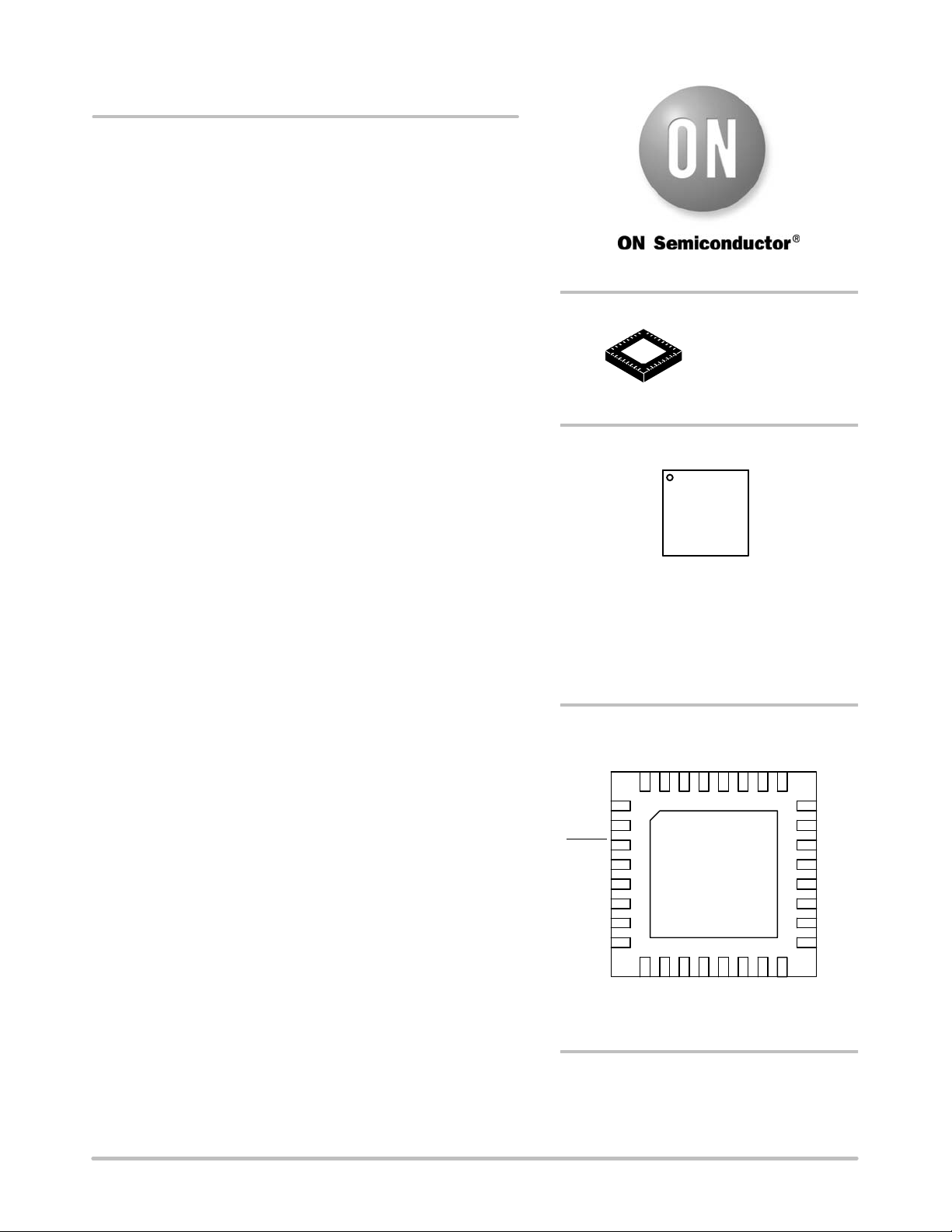
http://onsemi.com
QFN32
MN SUFFIX
CASE 488AM
See detailed ordering and shipping information in the package
dimensions section on page 31 of this data sheet.
ORDERING INFORMATION
32
1
ADP3211(A)
AWLYYWWG
G
1
(A) = ADP3211A Device Only
A = Assembly Location
WL = Wafer Lot
YY = Year
WW = Work Week
G = Pb−Free Package
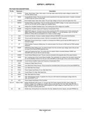
PIN ASSIGNMENT
MARKING DIAGRAM
VCC
BST
DRVH
SW
PVCC
DRVL
PGND
GND
EN
VID0
VID1
VID2
VID3
VID4
VID5
VID6
PWRGD
IMON
CLKEN
FBRTN
FB
COMP
GPU
ILIM
IREF
RPM
RT
RAMP
LLINE
CSREF
CSFB
CSCOMP
1
ADP3211
ADP3211A
(top view)
(Note: Microdot may be in either location)
Verzeichnis
- ・ Konfiguration des Pinbelegungsdiagramms on Seite 1 Seite 4
- ・ Abmessungen des Paketumrisses on Seite 32
- ・ Paket-Footprint-Pad-Layout on Seite 32
- ・ Teilenummerierungssystem on Seite 1 Seite 31 Seite 32
- ・ Markierungsinformationen on Seite 1
- ・ Blockdiagramm on Seite 2
- ・ Typisches Anwendungsschaltbild on Seite 21
- ・ Beschreibung der Funktionen on Seite 4
- ・ Technische Daten on Seite 1 Seite 3
- ・ Anwendungsbereich on Seite 1
- ・ Elektrische Spezifikation on Seite 5 Seite 6 Seite 7 Seite 8 Seite 9