
herunterladen
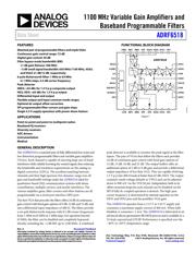
1100 MHz Variable Gain Amplifiers and
Baseband Programmable Filters
Data Sheet
ADRF6518
Rev. 0 Document Feedback
Information furnished by Analog Devices is believed to be accurate and reliable. However, no
responsibility is assumed by Analog Devices for its use, nor for any infringements of patents or other
rights of third parties that may result from its use. Specifications subject to change without notice. No
license is granted by implication or otherwise under any patent or patent rights of Analog Devices.
Trademarks and registered trademarks are the property of their respective owners.
One Technology Way, P.O. Box 9106, Norwood, MA 02062-9106, U.S.A.
Tel: 781.329.4700 ©2013 Analog Devices, Inc. All rights reserved.
Technical Support www.analog.com
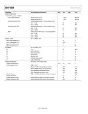
FEATURES
Matched pair of programmable filters and triple VGAs
Continuous gain control range: 72 dB
Digital gain control: 30 dB
Filter bypass mode bandwidth (BW)
±1 dB gain flatness: 300 MHz
−3 dB small signal bandwidth: 650 MHz/1100 MHz, VGA2
and VGA3 21 dB/12 dB, respectively
6-pole Butterworth filter: 1 MHz to 63 MHz
in 1 MHz steps, 0.5 dB corner frequency
Peak detector
IMD3: >65 dBc for 1.5 V p-p composite output
HD2, HD3: >65 dBc for 1.5 V p-p output
Differential input and output
Flexible output and input common-mode ranges
Optional dc output offset correction
SPI programmable filter corners and gain steps
Single 3.3 V supply operation with power-down feature
APPLICATIONS
Point-to-point and point-to-multipoint radios
Baseband IQ receivers
Diversity receivers
ADC drivers
Instrumentation
Medical
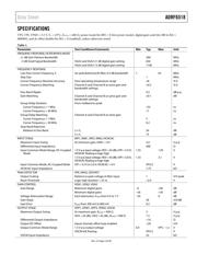
FUNCTIONAL BLOCK DIAGRAM
Figure 1
GENERAL DESCRIPTION
The ADRF6518 is a matched pair of fully differential low noise and
low distortion programmable filters and variable gain amplifiers
(VGAs). Each channel is capable of rejecting large out-of-band
interferers while reliably boosting the wanted signal, thus reducing
the bandwidth and resolution requirements on the analog-to-
digital converters (ADCs). The excellent matching between
channels and their high spurious-free dynamic range over all
gain and bandwidth settings make the ADRF6518 ideal for
quadrature-based (IQ) communication systems with dense
constellations, multiple carriers, and nearby interferers. The
various amplifier gains, filter corners and other features are all
programmable via a serial port interface (SPI) port.
The first VGA that precedes the filters offers 24 dB of continuous
gain control with fixed gain options of 9 dB, 12 dB, and 15 dB, and
sets a differential input impedance of 400 Ω. The filters provide
a six-pole Butterworth response with 0.5 dB corner frequencies
from 1 MHz to 63 MHz in 1 MHz steps. For operation beyond
63 MHz, the filter can be disabled and completely bypassed,
thereby extending the −3 dB BW up to 1100 MHz. A wideband
peak detector is available to monitor the peak signal at the filter
inputs. The pair of VGAs that follow the filters each provides
24 dB of continuous gain control with fixed gain options of
12 dB, 15 dB, 18 dB, and 21 dB. The output buffers offer an
additional option of 3 dB or 9 dB gain and provide a differential
output impedance of less than 10 Ω. They are capable of driving
1.5 V p-p into 400 Ω loads at better than 65 dBc HD3. The output
common-mode voltage defaults to VPS/2 and can be adjusted
down to 900 mV via the VOCM pin. Independent, built-in dc
offset correction loops for each channel can be disabled via the
SPI if fully dc-coupled operation is desired. The high-pass
corner frequency is determined by external capacitors on the
OFS1 and OFS2 pins and the postfilter VGA gain.
The ADRF6518 operates from a 3.15 V to 3.45 V supply and
consumes a maximum supply current of 400 mA. When fully
disabled, it consumes <1 mA. The ADRF6518 is fabricated in an
advanced silicon-germanium BiCMOS process and is available in a
32-lead, exposed pad LFCSP. Performance is specified over the
−40°C to +85°C temperature range.
ENBL
VPSD
COMD
LE
CLK
DATA
SDO/RST
VICM/AC
VPI
OPP1
OPM1
COM
VGN3
VOCM
COM
OPM2
OPP2
INP1 INM1 VPS
ADRF6518
RAVG VGN1 OFS1 VPS
COM INP2 INM2 VPS VPK VGN2 OFS2 VPS
SPI
11449-001
Verzeichnis
- ・ Konfiguration des Pinbelegungsdiagramms on Seite 8 Seite 40
- ・ Abmessungen des Paketumrisses on Seite 40
- ・ Teilenummerierungssystem on Seite 40
- ・ Blockdiagramm on Seite 1 Seite 22 Seite 35 Seite 36
- ・ Beschreibung der Funktionen on Seite 1 Seite 8 Seite 40
- ・ Technische Daten on Seite 1 Seite 4 Seite 7
- ・ Anwendungsbereich on Seite 1 Seite 22 Seite 27 Seite 28
- ・ Elektrische Spezifikation on Seite 9