
herunterladen
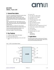
AS1355
300mA, Triple LDO
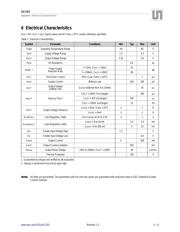
www.ams.com/LDOs/AS1355 Revision 1.3 1 - 12
1 General Description
The AS1355 is a high-performance triple CMOS low-dropout voltage
regulator in a single QFN package. The efficient set of
programmable power supplies is optimized to deliver the best
compromise between quiescent current and regulator performance
for mobile phones, PDAs, MP3 players, and other battery powered
devices.
Stability is guaranteed with ceramic output capacitors of only 1µF
(±20% – X5R) up to 4.7µF (±20% – X5R). The low equivalent series
resistance (ESR) of these capacitors ensures low output impedance
at high frequencies.
Regulation performance is excellent even under low dropout
conditions, when the power transistor has to operate in linear mode.
The low-noise performance allows direct connection of noise
sensitive circuits without additional filtering networks.
The AS1355 is available in a 16-pin QFN 3x3 package.
2 Key Features
3 Independent Voltage Regulators with Shutdown
Output Current: 300mA each LDO
Programmable Output Voltage Range: 1.25V to 3.6V in 50mV
Steps
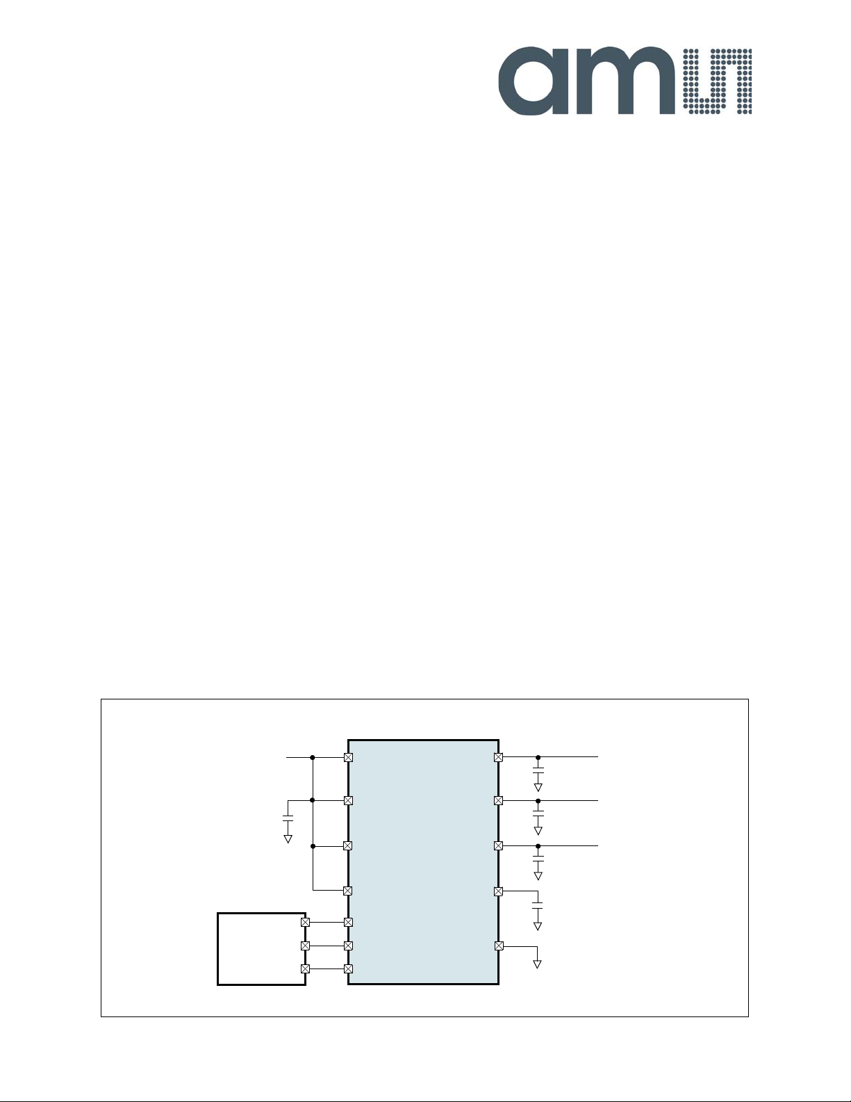
Figure 1. AS1355 - Typical Application Diagram
Accuracy: ±1.0%
PSRR: 70dB at 1kHz, 60dB at 100kHz
Load Regulation: 3mV (0 to 300mA)
Supply Range: 2.3V to 5.5V
0.1V Dropout Voltage @ Iload = 200mA
Shutdown Current: 1µA
Supply Current Without Load: 160µA
Softstart for Low Inrush Current
Stable with low ESR Ceramic Capacitors from 1µF to 4.7µF
Low Noise: 40µV rms @10Hz to 100kHz Bandwidth
Thermal Protection
Over-Current Protection
Temperature Range: -40°C to +85°C
Packages:
- 16-pin QFN 3x3
- 16-pin TQFN 3x3
3 Applications
The AS1355 is ideal for cordless and mobile phones, MP3 players,
CD and DVD players, PDAs, hand-held computers, digital cameras,
and any other hand-held battery-powered device.
1µF
3.3V
C
REF
= 100nF
(Improved Noise Performance)
µP
AS1355
VOUT1
VDD1
EN1
EN2
EN3
GND
REF
+5V
1µF
VDD2
VDD3
1µF
1.8V
VOUT2
1µF
1.5V
VOUT3
VDDA
Verzeichnis
- ・ Konfiguration des Pinbelegungsdiagramms on Seite 2
- ・ Abmessungen des Paketumrisses on Seite 9 Seite 10
- ・ Teilenummerierungssystem on Seite 11 Seite 12
- ・ Markierungsinformationen on Seite 9 Seite 10 Seite 11
- ・ Blockdiagramm on Seite 7
- ・ Typisches Anwendungsschaltbild on Seite 1 Seite 8
- ・ Beschreibung der Funktionen on Seite 1
- ・ Technische Daten on Seite 3
- ・ Anwendungsbereich on Seite 1 Seite 12
- ・ Elektrische Spezifikation on Seite 4