

herunterladen

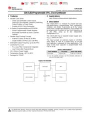
CDCEL824Ethernet PHY
USB Controller
WiFi
FPGA
25 MHz
Product
Folder
Sample &
Buy
Technical
Documents
Tools &
Software
Support &
Community
CDCEL824
SCAS945A ãJUNE 2015ãREVISED SEPTEMBER 2015
CDCEL824 Programmable 2-PLL Clock Synthesizer
1 Features 2 Applications
Laser Distance Measurement Applications
1
ã Flexible Clock Driver
ã Three User-Definable Control Inputs
3 Description
[S0/S1/S2]: for example, Frequency Switching,
The CDCEL824 is a modular PLL-based low-cost,
Output Enable, or Power Down
high-performance, programmable clock synthesizer,
ã Enables 0-PPM Clock Generation
multiplier, and divider. It generates up to four output
ã In-System Programmability and EEPROM
clocks from a single input frequency. Each output can
be programmed in-system for any clock frequency up
ã Serial Programmable Volatile Register
to 201 MHz, using up to two independent
ã Nonvolatile EEPROM to Store Customer
configurable PLLs.
Settings
The CDCEL824 has a separate output supply pins,
ã Flexible Input Clocking Concept
V
DDOUT
, which are 1.8 V.
ã External Crystal: 20 MHz to 30 MHz
The input accepts an external crystal or LVCMOS
ã Single-Ended LVCMOS up to 130 MHz
clock signal. In case of a crystal input, an on-chip
ã Selectable Output Frequency up to 201 MHz
load capacitor is adequate for most applications. The
value of the load capacitor is programmable from
ã Low-Noise PLL Core
0 pF to 20 pF.
ã PLL Loop Filter Components Integrated
ã Low Period Jitter (Typical 80 ps)
Device Information
(1)
ã 1.8-V Device Power Supply
PART NUMBER PACKAGE BODY SIZE (NOM)
ã Temperature Range ã40ô¯C to 85ô¯C
CDCEL824 TSSOP (16) 5.00 mm x 4.40 mm
ã Packaged in TSSOP
(1) For all available packages, see the orderable addendum at
the end of the data sheet.
Typical Schematic
1
An IMPORTANT NOTICE at the end of this data sheet addresses availability, warranty, changes, use in safety-critical applications,
intellectual property matters and other important disclaimers. PRODUCTION DATA.
Verzeichnis
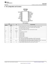
- У Konfiguration des Pinbelegungsdiagramms on Seite 3
- У Abmessungen des Paketumrisses on Seite 27 Seite 29 Seite 30
- У Markierungsinformationen on Seite 27
- У Blockdiagramm on Seite 1 Seite 9
- У Typisches Anwendungsschaltbild on Seite 22 Seite 23 Seite 24
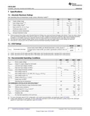
- У Technische Daten on Seite 4
- У Anwendungsbereich on Seite 1 Seite 33
- У Elektrische Spezifikation on Seite 6