


herunterladen
CDCE(L)9xx
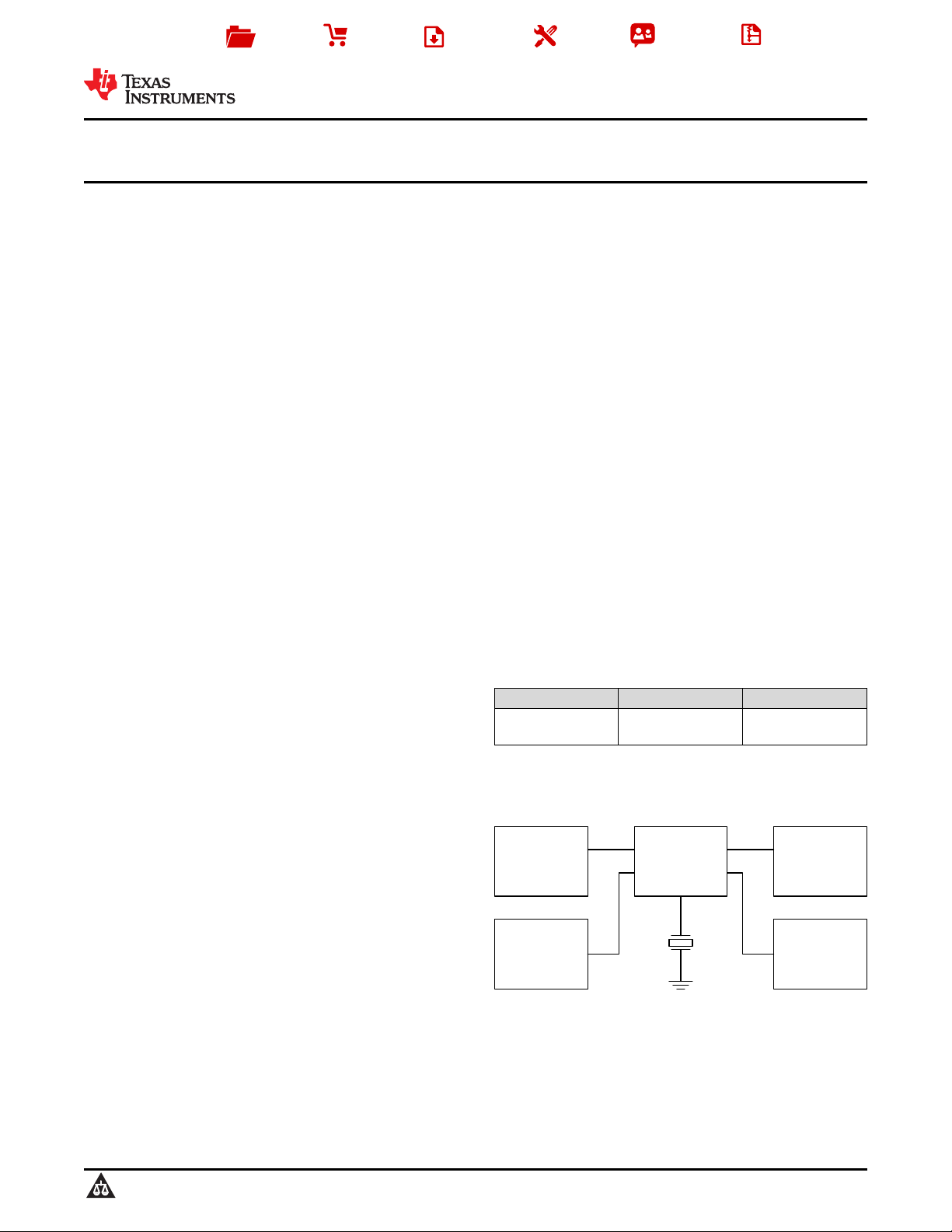
Clock
Ethernet
PHY
USB
Controller
WiFi
FPGA
25
MHz
Product
Folder
Sample &
Buy
Technical
Documents
Tools &
Software
Support &
Community
Reference
Design
CDCE913
,
CDCEL913
SCAS849F –JUNE 2007–REVISED APRIL 2015
CDCEx913 Programmable 1-PLL VCXO Clock Synthesizer
With 1.8-V, 2.5-V, and 3.3-V Outputs
1 Features 3 Description
The CDCE913 and CDCEL913 devices are modular
1
• Member of Programmable Clock Generator
PLL-based, low-cost, high-performance,
Family
programmable clock synthesizers. They generate up
– CDCE913/CDCEL913: 1-PLL, 3 Outputs
to three output clocks from a single input frequency.
– CDCE925/CDCEL925: 2-PLL, 5 Outputs
Each output can be programmed in-system for any
clock frequency up to 230 MHz, using the integrated
– CDCE937/CDCEL937: 3-PLL, 7 Outputs
configurable PLL.
– CDCE949/CDCEL949: 4-PLL, 9 Outputs
The CDCx913 has separate output supply pins,
• In-System Programmability and EEPROM
V
DDOUT
, which is 1.8 V for CDCEL913 and 2.5 V to
– Serial Programmable Volatile Register
3.3 V for CDCE913.
– Nonvolatile EEPROM to Store Customer
The input accepts an external crystal or LVCMOS
Settings
clock signal. A selectable on-chip VCXO allows
• Flexible Input Clocking Concept
synchronization of the output frequency to an external
control signal.
– External Crystal: 8 MHz to 32 MHz
– On-Chip VCXO: Pull Range ±150 ppm
The PLL supports SSC (spread-spectrum clocking)
for better electromagnetic interference (EMI)
– Single-Ended LVCMOS up to 160 MHz
performance.
• Free Selectable Output Frequency up to 230 MHz
The device supports nonvolatile EEPROM
• Low-Noise PLL Core
programming for easy customization of the device to
– PLL Loop Filter Components Integrated
the application. All device settings are programmable
– Low Period Jitter (Typical 50 ps)
through the SDA/SCL bus, a 2-wire serial interface.
• Separate Output Supply Pins
The CDCx913 operates in a 1.8-V environment. It
– CDCE913: 3.3 V and 2.5 V
operates in a temperature range of –40°C to 85°C.
– CDCEL913: 1.8 V
Device Information
(1)
• Flexible Clock Driver
PART NUMBER PACKAGE BODY SIZE (NOM)
– Three User-Definable Control Inputs
CDCE913
TSSOP (14) 5.00 mm × 4.40 mm
[S0/S1/S2], for Example, SSC Selection,
CDCEL913
Frequency Switching, Output Enable, or Power
(1) For all available packages, see the orderable addendum at
Down
the end of the data sheet.
– Generates Highly Accurate Clocks for Video,
Audio, USB, IEEE1394, RFID, Bluetooth
®
,
Typical Application Schematic
WLAN, Ethernet, and GPS
– Generates Common Clock Frequencies Used
With TI-DaVinci™, OMAP™, DSPs
– Programmable SSC Modulation
– Enables 0-PPM Clock Generation
• 1.8-V Device Power Supply
• Wide Temperature Range –40°C to 85°C
• Packaged in TSSOP
• Development and Programming Kit for Easy PLL
Design and Programming (TI Pro-Clock™)
2 Applications
D-TVs, STBs, IP-STBs, DVD Players, DVD
Recorders, and Printers
1
An IMPORTANT NOTICE at the end of this data sheet addresses availability, warranty, changes, use in safety-critical applications,
intellectual property matters and other important disclaimers. PRODUCTION DATA.
Verzeichnis
- ・ Konfiguration des Pinbelegungsdiagramms on Seite 3
- ・ Abmessungen des Paketumrisses on Seite 29 Seite 31 Seite 32
- ・ Markierungsinformationen on Seite 29 Seite 30
- ・ Blockdiagramm on Seite 1 Seite 10
- ・ Typisches Anwendungsschaltbild on Seite 1 Seite 20 Seite 21 Seite 22 Seite 23
- ・ Technische Daten on Seite 3 Seite 4
- ・ Anwendungsbereich on Seite 1 Seite 35
- ・ Elektrische Spezifikation on Seite 5 Seite 6