
herunterladen
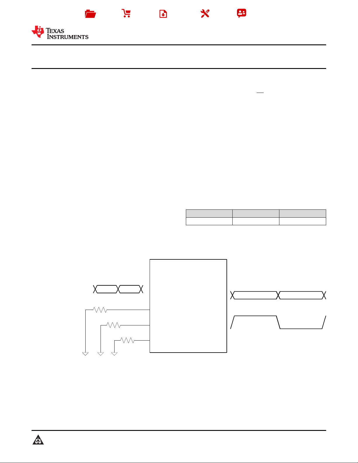
CDCM1802
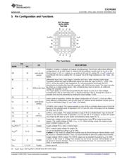
S0
S1
EN
R
EN
= 60lQ
R
S1
= 0
R
S0
= open
Setting for Mode 4:
EN = V
DD
/2
S1 = 0
S0 = 1
IN, IN
Y0,Y0
250 MHz
Y1
125 MHz
125 MHz
Product
Folder
Sample &
Buy
Technical
Documents
Tools &
Software
Support &
Community
CDCM1802
SCAS759B –APRIL 2004–REVISED NOVEMBER 2015
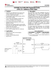
CDCM1802 Clock Buffer With Programmable Divider,
LVPECL I/O + Additional LVCMOS Output
1 Features 3 Description
The CDCM1802 clock driver distributes one pair of
1
• Distributes One Differential Clock Input to One
differential clock input to one LVPECL differential
LVPECL Differential Clock Output and One
clock output pair, Y0 and Y0, and one single-ended
LVCMOS Single-Ended Output
LVCMOS output, Y1. It is specifically designed for
• Programmable Output Divider for Both LVPECL
driving 50-Ω transmission lines. The LVCMOS output
and LVCMOS Outputs
is delayed by 1.6 ns over the PECL output stage to
minimize noise impact during signal transitions.
• 1.6-ns Output Skew Between LVCMOS and
LVPECL Transitions Minimizing Noise
The CDCM1802 has two control pins, S0 and S1, to
• 3.3-V Power Supply (2.5-V Functional)
select different output mode settings. The S[1:0] pins
are 3-level inputs. Additionally, an enable pin EN is
• Signaling Rate Up to 800-MHz LVPECL and
provided to disable or enable all outputs
200-MHz LVCMOS
simultaneously. The CDCM1802 is characterized for
• Differential Input Stage for Wide Common-Mode
operation from −40°C to 85°C.
Range Also Provides VBB Bias Voltage Output for
For single-ended driver applications, the CDCM1802
Single-Ended Input Signals
provides a VBB output pin that can be directly
• Receiver Input Threshold ±75 mV
connected to the unused input as a common-mode
• 16-Pin VQFN Package (3.00 mm × 3.00 mm)
voltage reference.
Device Information
(1)
2 Applications
PART NUMBER PACKAGE BODY SIZE (NOM)
• Networking and Data Communications
CDCM1802 VQFN (16) 3.00 mm × 3.00 mm
• Medical Imaging
(1) For all available packages, see the orderable addendum at
• Portable Test and Measurement
the end of the data sheet.
• High-end A/V
Application Example
1
An IMPORTANT NOTICE at the end of this data sheet addresses availability, warranty, changes, use in safety-critical applications,
intellectual property matters and other important disclaimers. PRODUCTION DATA.
Verzeichnis
- ・ Konfiguration des Pinbelegungsdiagramms on Seite 3
- ・ Abmessungen des Paketumrisses on Seite 23 Seite 25 Seite 26
- ・ Markierungsinformationen on Seite 23
- ・ Blockdiagramm on Seite 11 Seite 17
- ・ Typisches Anwendungsschaltbild on Seite 16 Seite 17 Seite 18
- ・ Technische Daten on Seite 4
- ・ Anwendungsbereich on Seite 1 Seite 30
- ・ Elektrische Spezifikation on Seite 5 Seite 6