

herunterladen
CY22800
Universal Programmable Clock Generator
(UPCG)
Cypress Semiconductor Corporation • 198 Champion Court • San Jose, CA 95134-1709 • 408-943-2600
Document #: 001-07704 Rev. *B Revised May 25, 2008
Features
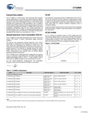
■ Spread Spectrum, VCXO, and Frequency Select
■ Input frequency range:
❐ Crystal: 8–30 MHz
❐ CLKIN: 0.5–100 MHz
■ Output frequency:
❐ Commercial: 1–200 MHz
❐ Industrial: 1–166 MHz
■ Integrated phase-locked loop
■ Low jitter, high accuracy outputs
■ 3.3V operation
■ 8-pin SOIC package
Benefits
■ Inventory of only one device, CY22800, is needed in various
applications such as HDTV, STB, DVDR, and so on.
■ Multiple predefined configurations that can be programmed
into a single chip.
■ Eliminates the need for expensive and difficult to use
higher-order crystal.
■ High-performance PLL tailored for multiple applications.
■ Meets critical timing requirements in complex system designs.
■ Enables application compatibility.
■ Allows up to three different frequency selects.
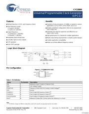
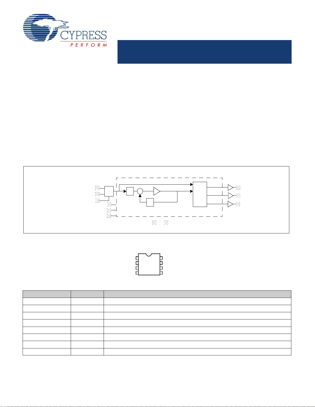
Pin Configuration
Figure 1. CY22800 8-Pin SOIC
XOUT
PLL
OSC
Q
P
VCO
VDD
VSS
Φ
CLKC
FS1
FS0
OUTPUT
DIVIDER
CLKB
(with modulation control)
XIN/CLKIN
CLKA
FS2
VCXO
Logic Block Diagram
1
2
3
4
XOUT
CLKB/FS1
VSS
CLKC/FS2/VSS
CLKA/FS0
5
6
7
8
VDD
XIN/CLKIN
FS0/VCXO
Table 1. Pin Definition
Name Pin Number Description
XIN 1 Reference Input; Crystal or External Clock
VDD 2 3.3V Voltage Supply
FS0/VCXO 3 Frequency Select 0/VCXO Analog Control Voltage
[1]
VSS 4 Ground
CLKB/FS1 5 Clock Output B/Frequency Select 1
[1]
CLKA/FS0 6 Clock Output A/Frequency Select 0
[1]
CLKC/FS2/VSS 7 Clock Output C/Frequency Select 2/VSS
[1]
XOUT 8 Reference Output (No Connect when the reference is a clock)
Note
1. Pin definition changes for different configurations. Refer to the specific one-page data sheet for more details.
[+] Feedback
Verzeichnis
- ・ Konfiguration des Pinbelegungsdiagramms on Seite 1
- ・ Teilenummerierungssystem on Seite 9
- ・ Blockdiagramm on Seite 1
- ・ Typisches Anwendungsschaltbild on Seite 8
- ・ Beschreibung der Funktionen on Seite 2
- ・ Technische Daten on Seite 7 Seite 8
- ・ Anwendungsbereich on Seite 4 Seite 7
- ・ Elektrische Spezifikation on Seite 8