
herunterladen
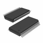
CY8C29466/CY8C29566
CY8C29666/CY8C29866
PSoC
®
Programmable System-on-Chip™
Cypress Semiconductor Corporation • 198 Champion Court • San Jose, CA 95134-1709 • 408-943-2600
Document Number: 38-12013 Rev. AB Revised August 12, 2015
PSoC
®
Programmable System-on-Chip™
Features
■ Powerful Harvard-architecture processor
❐ M8C processor speeds to 24 MHz
❐ Two 8 × 8 multiply, 32-bit accumulate
❐ Low power at high speed
❐ Operating voltage: 3.0 V to 5.25 V
❐ Operating voltages down to 1.0 V using on-chip switch mode
pump (SMP)
❐ Industrial temperature range: –40 °C to +85 °C
■ Advanced peripherals (PSoC
®
blocks)
❐ 12 rail-to-rail analog PSoC blocks provide:
• Up to 14-bit analog-to-digital converters (ADCs)
• Up to 9-bit digital-to-analog converters (DACs)
• Programmable gain amplifiers (PGAs)
• Programmable filters and comparators
❐ 16 digital PSoC blocks provide:
• 8- to 32-bit timers and counters, 8- and 16-bit pulse-width
modulators (PWMs)
• Cyclical redundancy check (CRC) and pseudo random
sequence (PRS) modules
• Up to four full-duplex universal asynchronous receiver
transmitters (UARTs)
• Multiple serial peripheral interface (SPI) masters or slaves
• Can connect to all general-purpose I/O (GPIO) pins
❐ Create complex peripherals by combining blocks
■ Precision, programmable clocking
❐ Internal ±5%
[1]
24- / 48-MHz main oscillator
❐ 24- / 48-MHz with optional 32.768 kHz crystal
❐ Optional external oscillator, up to 24 MHz
❐ Internal oscillator for watchdog and sleep
■ Flexible on-chip memory
❐ 32 KB flash program storage 50,000 erase/write cycles
❐ 2 KB static random access memory (SRAM) data storage
❐ In-system serial programming (ISSP)
❐ Partial flash updates
❐ Flexible protection modes
❐ Electrically erasable programmable read-only memory
(EEPROM) emulation in flash
■ Programmable pin configurations
❐ 25-mA sink, 10-mA source on all GPIOs
❐ Pull-up, pull-down, high Z, strong, or open-drain drive modes
on all GPIOs
❐ Eight standard analog inputs on GPIOs, plus four additional
analog inputs with restricted routing
❐ Four 40 mA analog outputs on GPIOs
❐ Configurable interrupt on all GPIOs
■ Additional system resources
❐ I
2
C slave, master, and multi-master to 400 kHz
❐ Watchdog and sleep timers
❐ User-configurable low-voltage detection (LVD)
❐ Integrated supervisory circuit
❐ On-chip precision voltage reference
■ Complete development tools
❐ Free development software (PSoC Designer™)
❐ Full-featured in-circuit emulator (ICE) and
programmer
❐ Full-speed emulation
❐ Complex breakpoint structure
❐ 128 KB trace memory
❐ Complex events
❐ C compilers, assembler, and linker
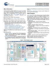
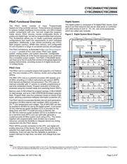
DIGITAL SYSTEM
SRAM
2KB
Interrupt
Controller
Sleep and
Watchdog
Multiple Clock Sources
(Includes IMO, ILO, PLL, and ECO)
Global Digital Interconnect
Global Analog Interconnect
PSoC
CORE
CPU Core (M8C)
SROM Flash 32KB
Digital
Block
Array
Multiply
Accum.
Switch
Mode
Pump
Internal
Voltage
Ref.
Digital
Clocks
POR and LVD
System Resets
Decimator
SYSTEM RESOURCES
ANALOG SYSTEM
Analog
Ref.
Analog
Input
Muxing
I
2
C
System Bus
Analog
Block
Array
Port
6
Port 0 with
Analog Drivers
Port
1
Port
2
Port
3
Port
4
Port
5
Port
7
Logic Block Diagram
Errata: For information on silicon errata, see “Errata” on page 61. Details include trigger conditions, devices affected, and proposed workaround.
Note
1. Errata: When the device is operated within 0 °C to 70 °C, the frequency tolerance is reduced to ±2.5%, but if operated at extreme temperature (below 0 °C or above
70 °C), frequency tolerance deviates from ±2.5% to ±5%. For more information, see Errata on page 61.
Verzeichnis
- ・ Abmessungen des Paketumrisses on Seite 47 Seite 48 Seite 49 Seite 50
- ・ Teilenummerierungssystem on Seite 54 Seite 61
- ・ Blockdiagramm on Seite 1 Seite 4 Seite 5
- ・ Schweißen Temperatur on Seite 51
- ・ Beschreibung der Funktionen on Seite 43
- ・ Technische Daten on Seite 21 Seite 22 Seite 23 Seite 24 Seite 25
- ・ Elektrische Spezifikation on Seite 21 Seite 22 Seite 38
- ・ Teilenummernliste on Seite 61