
herunterladen

PSoC
®
3: CY8C36
Automotive Family Datasheet
Programmable System-on-Chip (PSoC
®
)
Cypress Semiconductor Corporation • 198 Champion Court • San Jose, CA 95134-1709 • 408-943-2600
Document Number: 001-57330 Rev. *G Revised February 14, 2014
General Description
With its unique array of configurable blocks, PSoC
®
3 is a true system level solution providing microcontroller unit (MCU), memory,
analog, and digital peripheral functions in a single chip while being AEC-Q100 compliant. The CY8C36 family offers a modern method
of signal acquisition, signal processing, and control with high accuracy, high bandwidth, and high flexibility. Analog capability spans
the range from thermocouples (near DC voltages) to ultrasonic signals. The CY8C36 family can handle dozens of data acquisition
channels and analog inputs on every general-purpose input/output (GPIO) pin. The CY8C36 family is also a high-performance
configurable digital system with some part numbers including interfaces such as USB, multimaster inter-integrated circuit (I
2
C), and
controller area network (CAN). In addition to communication interfaces, the CY8C36 family has an easy to configure logic array, flexible
routing to all I/O pins, and a high-performance single cycle 8051 microprocessor core. You can easily create system-level designs
using a rich library of prebuilt components and boolean primitives using PSoC Creator™, a hierarchical schematic design entry tool.
The CY8C36 family provides unparalleled opportunities for analog and digital bill of materials integration while easily accommodating
last minute design changes through simple firmware updates.
Features
Single cycle 8051 CPU
DC to 67 MHz operation
Multiply and divide instructions
Flash program memory, up to 64 KB, 100,000 write cycles,
20 years retention, and multiple security features
512-byte flash cache
Up to 8-KB flash error correcting code (ECC) or configuration
storage
Up to 8 KB SRAM
Up to 2 KB electrically erasable programmable read-only
memory (EEPROM), 1 M cycles, and 20 years retention
24-channel direct memory access (DMA) with multilayer
AHB
[1]
bus access
• Programmable chained descriptors and priorities
• High bandwidth 32-bit transfer support
Low voltage, ultra low-power
Wide operating voltage range: 1.71 V to 5.5 V
0.8 mA at 3 MHz, 1.2 mA at 6 MHz, and 6.6 mA at 50 MHz
Low-power modes including:
• 1-µA sleep mode with real time clock and low-voltage
detect (LVD) interrupt
• 200-nA hibernate mode with RAM retention
Versatile I/O system
29 to 72 I/O (62 GPIOs, eight special input/outputs (SIO),
two USBIOs
[2]
)
Any GPIO to any digital or analog peripheral routability
LCD direct drive from any GPIO, up to 46 × 16 segments
[2]
CapSense
®
support from any GPIO
[3]
1.2-V to 5.5-V I/O interface voltages, up to four domains
Maskable, independent IRQ on any pin or port
Schmitt-trigger transistor-transistor logic (TTL) inputs
All GPIO configurable as open drain high/low, pull-up/
pull-down, High Z, or strong output
Configurable GPIO pin state at power-on reset (POR)
25 mA sink on SIO
Digital peripherals
20 to 24 programmable logic device (PLD) based universal
digital blocks (UDB)
Full CAN 2.0b 16 Rx, 8 Tx buffers
[2]
USB 2.0 certified Full-Speed (FS) 12 Mbps peripheral
interface (TID#40770053) using internal oscillator
[2]
Up to four 16-bit configurable timer, counter, and PWM blocks
67 MHz, 24-bit fixed point digital filter block (DFB) to
implement FIR and IIR filters
Library of standard peripherals
• 8-, 16-, 24-, and 32-bit timers, counters, and PWMs
• Serial peripheral interface (SPI), universal asynchronous
transmitter receiver (UART), and I
2
C
• Many others available in catalog
Library of advanced peripherals
• Cyclic redundancy check (CRC)
• Pseudo random sequence (PRS) generator
• Local interconnect network (LIN) bus 2.0
• Quadrature decoder
Analog peripherals (1.71 V VDDA 5.5 V)
1.024 V ± 0.1% internal voltage reference across –40 °C to
+85 °C
Configurable delta-sigma ADC with 8- to 12-bit resolution
• Sample rates up to 192 ksps
• Programmable gain stage: ×0.25 to ×16
• 12-bit mode, 192 ksps, 66-dB signal to noise and distortion
ratio (SINAD), ±1-bit INL/DNL
Up to four 8-bit, 8-Msps IDACs or 1-Msps VDACs
Four comparators with 95-ns response time
Up to four uncommitted opamps with 25-mA drive capability
Up to four configurable multifunction analog blocks. Example
configurations are programmable gain amplifier (PGA),
transimpedance amplifier (TIA), mixer, and sample and hold
CapSense support
Programming, debug, and trace
JTAG (4-wire), serial wire debug (SWD) (2-wire), and single
wire viewer (SWV) interfaces
Eight address and one data breakpoint
4-KB instruction trace buffer
Bootloader programming supportable through I
2
C, SPI,
UART, USB, and other interfaces
Precision, programmable clocking
3- to 62-MHz internal oscillator over full temperature and
voltage range
4- to 25-MHz crystal oscillator for crystal PPM accuracy
Internal PLL clock generation up to 67 MHz
32.768-kHz watch crystal oscillator
Low-power internal oscillator at 1, 33, and 100 kHz
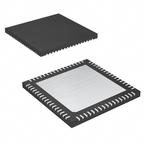
Temperature and packaging
–40 °C to +85 °C degrees automotive temperature
–40 °C to +125 °C Extended temperature range
48-pin SSOP, and 100-pin TQFP package options
AEC-Q100 compliant.
Notes
1. AHB – AMBA (advanced microcontroller bus architecture) high-performance bus, an ARM data transfer bus
2. This feature on select devices only. See Ordering Information on page 133 for details.
3. GPIOs with opamp outputs are not recommended for use with CapSense.
Verzeichnis
- ・ Konfiguration des Pinbelegungsdiagramms on Seite 9 Seite 22 Seite 95
- ・ Abmessungen des Paketumrisses on Seite 135 Seite 136
- ・ Teilenummerierungssystem on Seite 1 Seite 4 Seite 133 Seite 134
- ・ Blockdiagramm on Seite 3 Seite 8 Seite 23 Seite 28 Seite 34
- ・ Schweißen Temperatur on Seite 135
- ・ Beschreibung der Funktionen on Seite 1 Seite 26 Seite 43 Seite 52 Seite 54
- ・ Technische Daten on Seite 4 Seite 39 Seite 50 Seite 60 Seite 65
- ・ Anwendungsbereich on Seite 60
- ・ Elektrische Spezifikation on Seite 4 Seite 50 Seite 65