
herunterladen

DAC
GND
DACx760
AVDDDVDD-EN
AVSS
DVDD
Pre-
Conditioning
Current
Source
I
ENABLE
ISET-R
I
GAIN
V
GAIN
V
ENABLE
Current Output Stage
Voltage Output Stage
Watchdog
Timer
Slew Rate
Control
User Calibration
Gain/Offset
Register
DAC Input
Register
Thermal
Alarm
Internal
Reference
SPI Shift Register
Input Control Logic
Control Logic
CMP
–VSENSE
+VSENSE
VOUT
IOUT
ALARM
BOOST
REFOUT
REFIN HART-IN
LATCH
SCLK
DIN
SDO
CLR
CLR-SEL
Copyright © 2016, Texas Instruments Incorporated
Product
Folder
Sample &
Buy
Technical
Documents
Tools &
Software
Support &
Community
Reference
Design
An IMPORTANT NOTICE at the end of this data sheet addresses availability, warranty, changes, use in safety-critical applications,
intellectual property matters and other important disclaimers. PRODUCTION DATA.
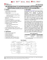
DAC7760
,
DAC8760
SBAS528B –JUNE 2013–REVISED JUNE 2016
DACx760 Single-Channel, 12- and 16-Bit Programmable Current and Voltage Output
Digital-to-Analog Converters for 4-mA to 20-mA Current Loop Applications
1
1 Features
1
• Current Output: 4 mA to 20 mA;
0 mA to 20 mA; 0 mA to 24 mA
• Voltage Output:
– 0 V to 5 V; 0 V to 10 V; ±5 V; ±10 V
– 0 V to 5.5 V; 0 V to 11 V; ±5.5 V; ±11 V
(10% Over Range)
• ±0.1% FSR Total Unadjusted Error (TUE)
Maximum
• DNL: ±1 LSB Maximum
• Simultaneous Voltage and Current Output
• Internal 5-V Reference (10 ppm/°C, Maximum)
• Internal 4.6-V Power-Supply Output
• Reliability Features:
– CRC Check and Watchdog Timer
– Thermal Alarm
– Open Alarm, Short Current Limit
• Wide Temperature Range: –40°C to 125°C
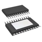
• 6-mm × 6-mm 40-Pin VQFN and 24-Pin HTSSOP
Packages
2 Applications
• 4-mA to 20-mA Current Loops
• Analog Output Modules
• Building Automation
• Environment Monitoring
• Programmable Logic Controllers (PLCs)
• Field Sensors and Process Transmitters
3 Description
The DAC7760 and DAC8760 are low-cost, precision,
fully-integrated, 12-bit and 16-bit digital-to-analog
converters (DACs) designed to meet the
requirements of industrial process-control
applications. These devices can be programmed as a
current output with a range of 4 mA to 20 mA, 0 mA
to 20 mA, or 0 mA to 24 mA; or as a voltage output
with a range of 0 V to 5 V, 0 V to 10 V, ±5 V, or
±10 V with a 10% overrange (0 V to 5.5 V, 0 V to
11 V, ±5.5 V, or ±11 V). Both current and voltage
outputs can be simultaneously enabled while being
controlled by a single data register.
These devices include a power-on-reset function to
ensure powering up in a known state (both IOUT and
VOUT are disabled and in a Hi-Z state). The CLR
and CLR-SEL pins set the voltage outputs to zero-
scale or midscale, and the current output to the low
end of the range, if the output is enabled. Zero and
gain registers can be programmed to digitally
calibrate the device in the end system. The output
slew rate is also programmable by register. These
devices can superimpose an external HART
®
signal
on the current output and can operate with either a
single 10-V to 36-V supply, or dual supplies of up to
±18 V. All versions are available in both 6-mm ×
6-mm 40-pin VQFN and 24-pin HTSSOP packages.
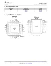
Device Information
(1)
PART NUMBER PACKAGE BODY SIZE (NOM)
DACx760
HTSSOP (24) 7.80 mm × 4.40 mm
VQFN (40) 6.00 mm × 6.00 mm
(1) For all available packages, see the orderable addendum at
the end of the data sheet.
Block Diagram
Verzeichnis
- ・ Konfiguration des Pinbelegungsdiagramms on Seite 3 Seite 4
- ・ Abmessungen des Paketumrisses on Seite 53 Seite 55 Seite 56
- ・ Markierungsinformationen on Seite 53 Seite 54
- ・ Blockdiagramm on Seite 1 Seite 26
- ・ Typisches Anwendungsschaltbild on Seite 47 Seite 48 Seite 49
- ・ Technische Daten on Seite 5 Seite 51
- ・ Anwendungsbereich on Seite 1 Seite 63
- ・ Elektrische Spezifikation on Seite 6 Seite 7 Seite 8 Seite 9 Seite 10