


herunterladen
© Semiconductor Components Industries, LLC, 2015
December, 2015 − Rev. 8
1 Publication Order Number:
NCP1612/D
NCP1612A, NCP1612B,
NCP1612A1, NCP1612A2,
NCP1612B2
Enhanced, High‐Efficiency
Power Factor Controller
The NCP1612 is designed to drive PFC boost stages based on an
innovative Current Controlled Frequency Fold-back (CCFF) method.
In this mode, the circuit classically operates in Critical conduction
Mode (CrM) when the inductor current exceeds a programmable
value. When the current is below this preset level, the NCP1612
linearly decays the frequency down to about 20 kHz when the current
is null. CCFF maximizes the efficiency at both nominal and light load.
In particular, the stand-by losses are reduced to a minimum.
Like in FCCrM controllers, an internal circuitry allows near-unity
power factor even when the switching frequency is reduced. Housed in
a SO−10 package, the circuit also incorporates the features necessary
for robust and compact PFC stages, with few external components.
General Features
• Near-unity Power Factor
• Critical Conduction Mode (CrM)
• Current Controlled Frequency Fold-back (CCFF): Low Frequency
Operation is Forced at Low Current Levels
• On-time Modulation to Maintain a Proper Current Shaping in CCFF
Mode
• Skip Mode Near the Line Zero Crossing
• Fast Line/Load Transient Compensation
(Dynamic Response Enhancer)
• Valley Turn On
• High Drive Capability: −500 mA/+800 mA
• V
CC
Range: from 9.5 V to 35 V
• Low Start-up Consumption
• 5 Versions: NCP1612A, B, A1, A2 and B2 (see Table 1)
• Line Range Detection
• pfcOK Signal
• This is a Pb-Free Device
Safety Features
• Separate Pin for Fast Over-voltage Protection (FOVP)
for Redundancy
• Soft Over-voltage Protection
• Brown-out Detection
• Soft-start for Smooth Start-up Operation
(A, A1 and A2 Versions)
• Over Current Limitation
• Disable Protection if the Feedback is Not Connected
• Thermal Shutdown
• Latched Off Capability
• Low Duty-cycle Operation if the Bypass Diode is
shorted
• Open Ground Pin Fault Monitoring
• Saturated Inductor Protection
• Detailed Safety Testing Analysis
(Refer to Application Note AND9079/D
)
Typical Applications
• PC Power Supplies
• All Off Line Appliances Requiring Power Factor
Correction
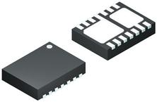
SOIC−10
CASE 751BQ
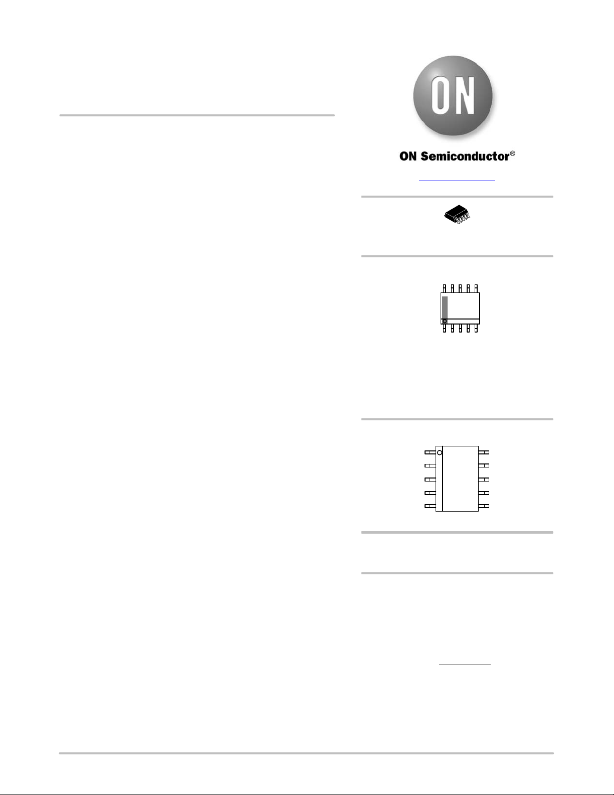
PIN CONNECTIONS
MARKING DIAGRAM
(Top View)
www.onsemi.com
1612x = Specific Device Code
x = A, A1, A2, B or B2
A = Assembly Location
L = Wafer Lot
Y = Year
W = Work Week
G = Pb-Free Package
See detailed ordering and shipping information in the package
dimensions section on page 30 of this data sheet.
ORDERING INFORMATION
1612x
ALYW
G
1
10
pfcOK
V
CC
DRV
GND
FOVP
1
CS/ZCD
V
control
V
sense
Feedback
FFcontrol
Verzeichnis
- ・ Konfiguration des Pinbelegungsdiagramms on Seite 1 Seite 7
- ・ Abmessungen des Paketumrisses on Seite 31
- ・ Paket-Footprint-Pad-Layout on Seite 31
- ・ Teilenummerierungssystem on Seite 1 Seite 30 Seite 31
- ・ Markierungsinformationen on Seite 1 Seite 30 Seite 31
- ・ Blockdiagramm on Seite 2 Seite 8
- ・ Typisches Anwendungsschaltbild on Seite 1 Seite 2
- ・ Technische Daten on Seite 30
- ・ Anwendungsbereich on Seite 1 Seite 2
- ・ Elektrische Spezifikation on Seite 4 Seite 5 Seite 6
- ・ Teilenummernliste on Seite 3