


herunterladen
©2008 Fairchild Semiconductor Corporation 1 www.fairchildsemi.com
FDB52N20 Rev. C1
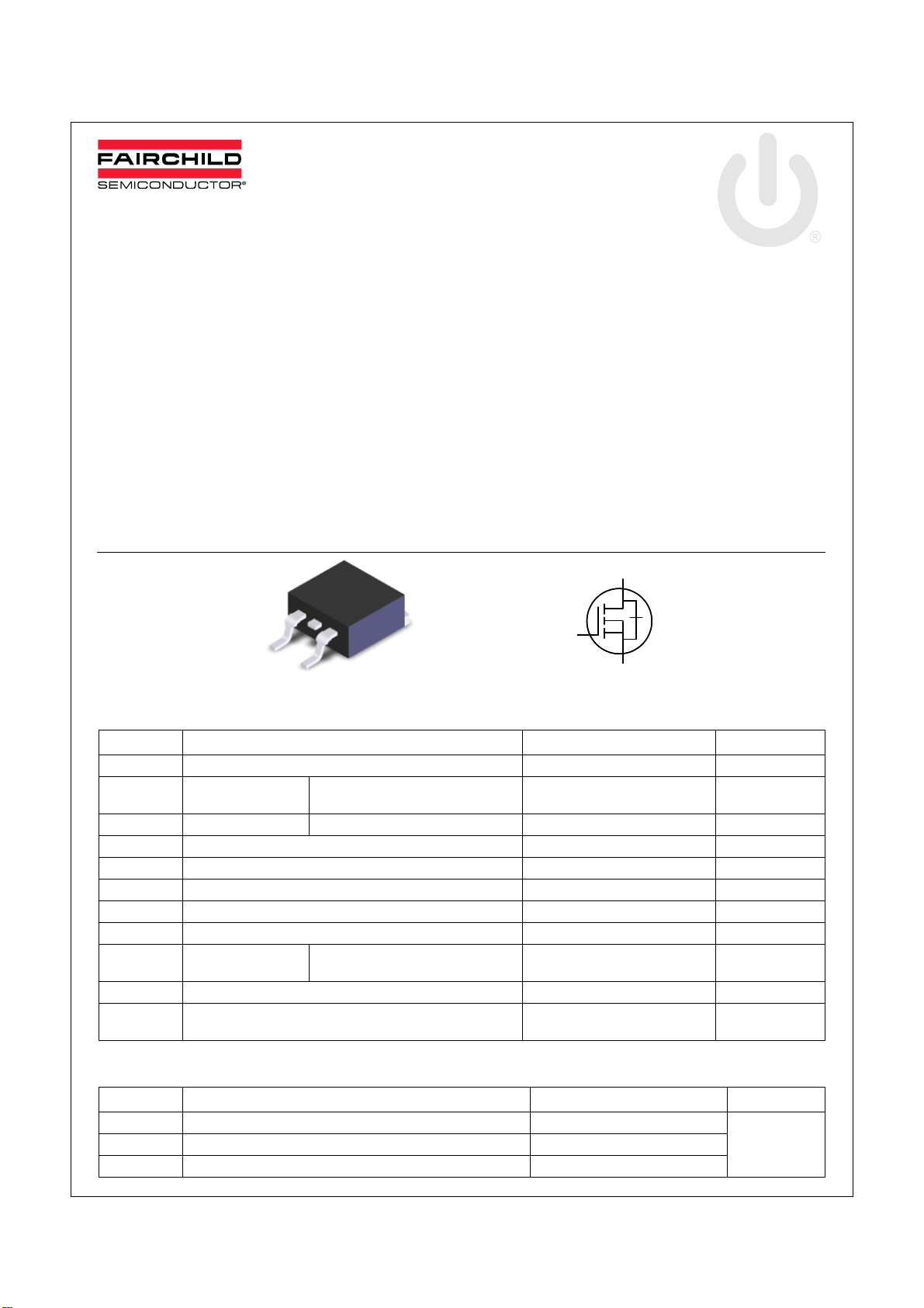
FDB52N20 N-Channel UniFET
TM
MOSFET
May 2013
FDB52N20
N-Channel UniFET
TM
MOSFET
200 V, 52 A, 49 m
Features
•R
DS(on)
= 49 m (Max.) V
GS
= 10 V, I
D
= 26 A
• Low Gate Charge (Typ. 49 nC)
•Low C
rss
(Typ. 66 pF)
• 100% Avalanche Tested
Applications
•PDP TV
• Lighting
• Uninterruptible Power Supply
• AC-DC Power Supply
Description
UniFET
TM
MOSFET is Fairchild Semiconductor
®
’s high voltage
MOSFET family based on planar stripe and DMOS technology.
This MOSFET is tailored to reduce on-state resistance, and to
provide better switching performance and higher avalanche
energy strength. This device family is suitable for switching
power converter applications such as power factor correction
(PFC), flat panel display (FPD) TV power, ATX and electronic
lamp ballasts.
Absolute Maximum Ratings
Thermal Characteristics
* When mounted on the minimum pad size recommended (PCB Mount)
S
D
G
G
S
D
D
2
-PAK
Symbol Parameter FDB52N20 Unit
V
DSS
Drain-Source Voltage 200 V
I
D
Drain Current - Continuous (T
C
= 25C)
- Continuous (T
C
= 100C)
52
33
A
A
I
DM
Drain Current - Pulsed
(Note 1)
208 A
V
GSS
Gate-Source voltage 30 V
E
AS
Single Pulsed Avalanche Energy
(Note 2)
2520 mJ
I
AR
Avalanche Current
(Note 1)
52 A
E
AR
Repetitive Avalanche Energy
(Note 1)
35.7 mJ
dv/dt Peak Diode Recovery dv/dt
(Note 3)
4.5 V/ns
P
D
Power Dissipation (T
C
= 25C)
- Derate above 25C
357
2.86
W
W/C
T
J,
T
STG
Operating and Storage Temperature Range -55 to +150 C
T
L
Maximum Lead Temperature for Soldering Purpose,
1/8” from Case for 5 Seconds
300 C
Symbol Parameter FDB52N20 Unit
R
JC
Thermal Resistance, Junction-to-Case, Max. 0.35
C/WR
JA
* Thermal Resistance, Junction-to-Ambient*, Max. 40
R
JA
Thermal Resistance, Junction-to-Ambient, Max. 62.5
Verzeichnis