

herunterladen
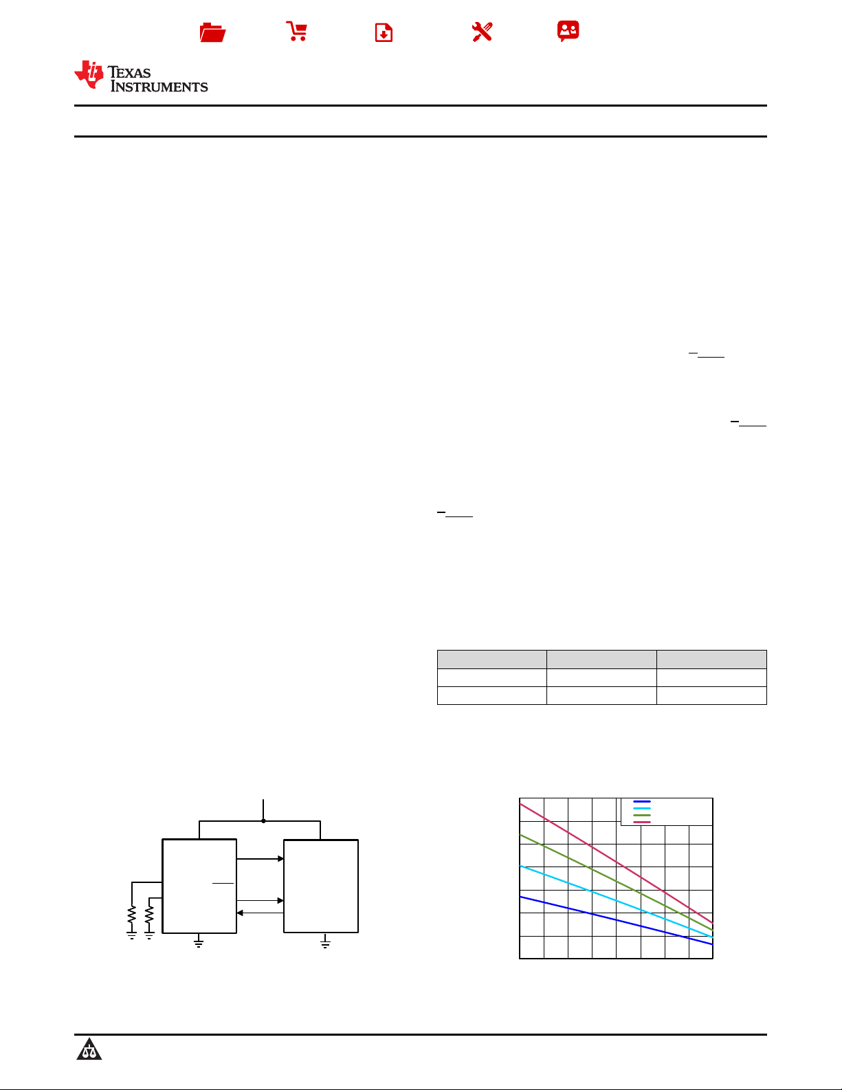
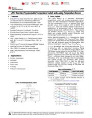
0
500
1,000
1,500
2,000
2,500
3,000
3,500
-50 -25 0 25 50 75 100 125 150
VTEMP VOLTAGE (mV)
TEMPERTURE (C)
J2 (-5.166mV/°C)
J3 (-7.752mV/°C)
J4 (-10.339mV/°C)
J5 (-12.924mV/°C)
C101
V
DD
Supply
(+2.4V to +5.5V)
GND
V
DD
T
OVER
V
TEMP
TRIP TEST
Microcontroller
LM57
ADC Input
T
OVER
Digital In
Digital Out
SENSE1
SENSE2
Analog
R
SENSE1
R
SENSE2
Product
Folder
Sample &
Buy
Technical
Documents
Tools &
Software
Support &
Community
LM57
SNIS152E –MAY 2009–REVISED JULY 2015
LM57 Resistor-Programmable Temperature Switch and Analog Temperature Sensor
1 Features 3 Description
The LM57 device is a precision, dual-output,
1
• See LM57-Q1 Data Sheet for AEC-Q100 Grade
temperature switch with analog temperature sensor
1/Grade 0/Grade 0 Extended (Qualified and
output for wide temperature industrial applications.
Manufactured on an Automotive Grade Flow)
The trip temperature (T
TRIP
) is selected from 256
• Trip Temperature Set by External Resistors with
possible values in the range of –40°C to 150°C. The
Accuracy of ±1.7°C or ±2.3°C from −40°C to
V
TEMP
is a class AB analog voltage output that is
+150°C
proportional to temperature with a programmable
negative temperature coefficient (NTC). Two external
• Resistor Tolerance Contributes Zero Error
1% resistors set the T
TRIP
and V
TEMP
slope. The
• Push-Pull and Open-Drain Switch Outputs
digital and analog outputs enable protection and
• Wide Operating Temperature Range of −50°C to
monitoring of system thermal events.
150°C
Built-in thermal hysteresis (T
HYST
) prevents the digital
• Very Linear Analog V
TEMP
Temp Sensor Output
outputs from oscillating. The T
OVER
and T
OVER
digital
with ±0.8°C or ±1.3°C Accuracy from −50°C to
outputs will assert when the die temperature exceeds
+150°C
T
TRIP
and will de-assert when the temperature falls
below a temperature equal to T
TRIP
minus T
HYST
.
• Short-Circuit Protected Analog and Digital Outputs
• Latching Function for Digital Outputs
T
OVER
is active-high with a push-pull structure. T
OVER
is active-low with an open-drain structure. Tying
• TRIP-TEST Pin Allows In-System Testing
T
OVER
to TRIP-TEST will latch the output after it trips.
• Low Power Minimizes Self-Heating to Under
The output can be cleared by forcing TRIP-TEST low.
0.02°C
Driving the TRIP-TEST high will assert the digital
outputs. A processor can check the state of T
OVER
or
2 Applications
T
OVER
, confirming they changed to an active state.
This allows for in situ verification that the comparator
• Factory Automation
and output circuitry are functional after system
• Industrial
assembly. When TRIP-TEST is high, the trip-level
• Automotive
reference voltage appears at the V
TEMP
pin. The
system could then use this voltage to calculate the
• Down Hole
threshold of the LM57.
• Avionics
• Telecom Infrastructure
Device Information
(1) (2)
PART NUMBER PACKAGE BODY SIZE (NOM)
LM57BISD WSON (8) 2.50 mm × 2.50 mm
LM57FPW TSSOP (8) 3.00 mm × 6.40 mm
(1) For all available packages, see the orderable addendum at
the end of the data sheet.
(2) For device comparison see Device Comparison Table .
LM57 Overtemperature Alarm
Temperature Transfer Function
1
An IMPORTANT NOTICE at the end of this data sheet addresses availability, warranty, changes, use in safety-critical applications,
intellectual property matters and other important disclaimers. PRODUCTION DATA.
Verzeichnis
- ・ Konfiguration des Pinbelegungsdiagramms on Seite 4 Seite 5
- ・ Abmessungen des Paketumrisses on Seite 32 Seite 34 Seite 35 Seite 37
- ・ Paket-Footprint-Pad-Layout on Seite 38
- ・ Markierungsinformationen on Seite 32 Seite 33
- ・ Blockdiagramm on Seite 12 Seite 26 Seite 28
- ・ Typisches Anwendungsschaltbild on Seite 22 Seite 26 Seite 27 Seite 28
- ・ Schweißen Temperatur on Seite 5
- ・ Technische Daten on Seite 5
- ・ Anwendungsbereich on Seite 1 Seite 22 Seite 40
- ・ Elektrische Spezifikation on Seite 7 Seite 8 Seite 9 Seite 27