

herunterladen
© Semiconductor Components Industries, LLC, 2014
June, 2014 − Rev. 2
1 Publication Order Number:
MC100EP196B/D
MC100EP196B
3.3 V ECL Programmable
Delay Chip With FTUNE
Descriptions
The MC100EP196B is a Programmable Delay Chip (PDC) designed
primarily for clock deskewing and timing adjustment. It provides variable
delay of a differential NECL/PECL input transition. It has similar
architecture to the EP195 with the added feature of further tunability in
delay using the FTUNE pin. The FTUNE input takes an analog voltage
from V
CC
to V
EE
to fine tune the output delay from 0 to 60 ps.
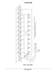
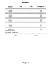
The delay section consists of a programmable matrix of gates and
multiplexers as shown in the logic diagram, Figure 3. The delay
increment of the EP196B has a digitally selectable resolution of about
10 ps and a net range of up to 10.4 ns. The required delay is selected by
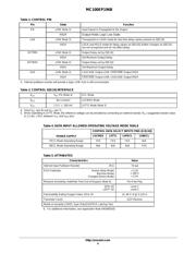
the 10 data select inputs D[9:0] values and controlled by the LEN
(Pin 10). A LOW level on LEN allows a transparent LOAD mode of
real time delay values by D[9:0]. A LOW to HIGH transition on LEN
will LOCK and HOLD current values present against any subsequent
changes in D[10:0]. The approximate delay values for varying tap
numbers correlating to D0 (LSB) through D9 (MSB) are shown in
Table 6 and Figure 4.
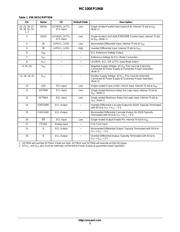
The IN/IN
inputs can accept LVPECL (SE or Diff), or LVDS level
signals. Because the MC100EP196B is designed using a chain of
multiplexers it has a fixed minimum delay of 2.2 ns. An additional pin
D10 is provided for controlling Pins 14 and 15, CASCADE and
CASCADE
, also latched by LEN, in cascading multiple PDCs for
increased programmable range. The cascade logic allows full control of
multiple PDCs. Switching devices from all “1” states on D[0:9] with
SETMAX LOW to all “0” states on D[0:9] with SETMAX HIGH will
increase the delay equivalent to “D0”, the minimum increment.
Select input pins D[10:0] may be threshold controlled by
combinations of interconnects between V
EF
(pin 7) and V
CF
(pin 8) for
receiving LVCMOS, ECL, or LVTTL level signals. For LVCMOS input
levels, leave V
CF
and V
EF
open. For ECL operation, short V
CF
and V
EF
(Pins 7 and 8). For LVTTL level operation, connect a 1.5 V supply
reference to V
CF
and leave open V
EF
pin. The 1.5 V reference voltage at
the V
CF
pin can be accomplished by placing a 2.2 kW resistor between
V
CF
and V
EE
for a 3.3 V power supply.
The V
BB
pin, an internally generated voltage supply, is available to
this device only. For single−ended input conditions, the unused
differential input is connected to V
BB
as a switching reference voltage.
V
BB
may also rebias AC coupled inputs. When used, decouple V
BB
and
V
CC
via a 0.01 mF capacitor and limit current sourcing or sinking to
0.5 mA. When not used, V
BB
should be left open.
The 100 Series contains temperature compensation.
Features
• Maximum Input Clock Frequency >1.2 GHz Typical
• Programmable Range: 0 ns to 10 ns
• Delay Range: 2.2 ns to 12.4 ns
• 10 ps Increments
• Linearity ±40 ps max
• PECL Mode Operating Range:
V
CC
= 3.0 V to 3.6 V with V
EE
= 0 V
• NECL Mode Operating Range:
V
CC
= 0 V with V
EE
= −3.0 V to −3.6 V
• IN/IN Inputs Accept LVPECL, LVNECL, LVDS Levels
• A Logic High on the EN Pin Will Force Q to Logic Low
• D[10:0] Can Select Either LVPECL, LVCMOS, or
LVTTL Input Levels
• V
BB
Output Reference Voltage
• These are Pb−Free Devices
MARKING
DIAGRAMS*
*For additional marking information, refer to
Application Note AND8002/D.
http://onsemi.com
See detailed ordering and shipping information in the package
dimensions section on page 16 of this data sheet.
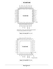
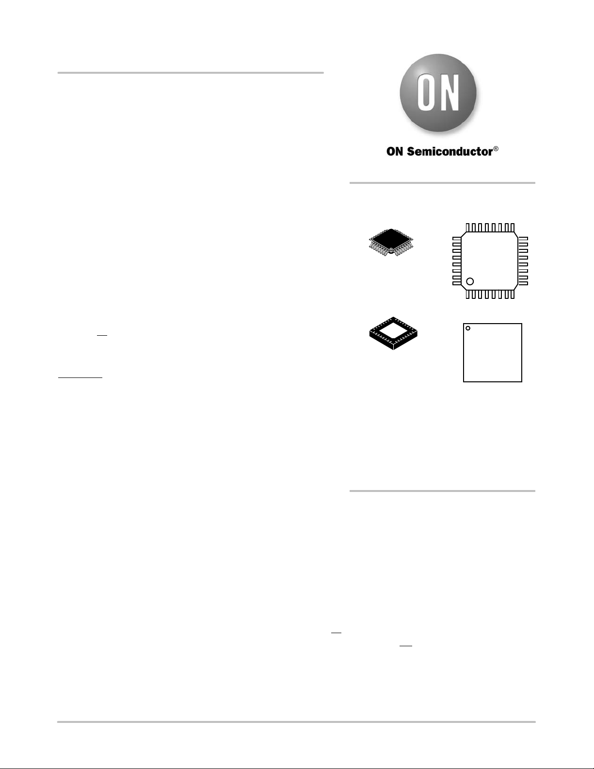
ORDERING INFORMATION
QFN32
MN SUFFIX
CASE 488AM
32
1
32
1
MC100
EP196B
AWLYYWWG
LQFP−32
FA SUFFIX
CASE 873A
A = Assembly Location
WL, L = Wafer Lot
Y, YY = Year
W, WW = Work Week
G or G = Pb−Free Package
MC100
EP196B
ALYWG
G
1
(Note: Microdot may be in either location)
Verzeichnis
- ・ Konfiguration des Pinbelegungsdiagramms on Seite 3
- ・ Abmessungen des Paketumrisses on Seite 17 Seite 18
- ・ Paket-Footprint-Pad-Layout on Seite 18
- ・ Teilenummerierungssystem on Seite 1 Seite 16 Seite 18
- ・ Markierungsinformationen on Seite 1 Seite 16 Seite 18
- ・ Blockdiagramm on Seite 13
- ・ Typisches Anwendungsschaltbild on Seite 5 Seite 11
- ・ Technische Daten on Seite 16