
herunterladen
© Semiconductor Components Industries, LLC, 2014
June, 2014 − Rev. 19
1 Publication Order Number:
MC10EP195/D
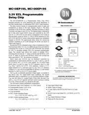
MC10EP195, MC100EP195
3.3V ECL Programmable
Delay Chip
The MC10/100EP195 is a Programmable Delay Chip (PDC)
designed primarily for clock deskewing and timing adjustment. It
provides variable delay of a differential NECL/PECL input transition.
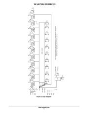
The delay section consists of a programmable matrix of gates and
multiplexers as shown in the logic diagram, Figure 3. The delay
increment of the EP195 has a digitally selectable resolution of about
10 ps and a net range of up to 10.2 ns. The required delay is selected by
the 10 data select inputs D[9:0] values and controlled by the LEN
(pin 10). A LOW level on LEN allows a transparent LOAD mode of
real time delay values by D[9:0]. A LOW to HIGH transition on LEN
will LOCK and HOLD current values present against any subsequent
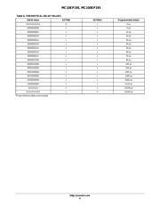
changes in D[10:0]. The approximate delay values for varying tap
numbers correlating to D0 (LSB) through D9 (MSB) are shown in
Table 6 and Figure 4.
Because the EP195 is designed using a chain of multiplexers it has a
fixed minimum delay of 2.2 ns. An additional pin D10 is provided for
controlling Pins 14 and 15, CASCADE and CASCADE
, also latched
by LEN, in cascading multiple PDCs for increased programmable
range. The cascade logic allows full control of multiple PDCs.
Switching devices from all “1” states on D[0:9] with SETMAX LOW
to all “0” states on D[0:9] with SETMAX HIGH will increase the
delay equivalent to “D0”, the minimum increment.
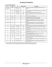
Select input pins D[10:0] may be threshold controlled by
combinations of interconnects between V
EF
(pin 7) and V
CF
(pin 8)
for LVCMOS, ECL, or LVTTL level signals. For LVCMOS input
levels, leave V
CF
and V
EF
open. For ECL operation, short V
CF
and
V
EF
(Pins 7 and 8). For LVTTL level operation, connect a 1.5 V
supply reference to V
CF
and leave open V
EF
pin. The 1.5 V reference
voltage to V
CF
pin can be accomplished by placing a 2.2 kW resistor
between V
CF
and V
EE
for a 3.3 V power supply.
The V
BB
pin, an internally generated voltage supply, is available to
this device only. For single−ended input conditions, the unused
differential input is connected to V
BB
as a switching reference voltage.
V
BB
may also rebias AC coupled inputs. When used, decouple V
BB
and V
CC
via a 0.01 mF capacitor and limit current sourcing or sinking
to 0.5 mA. When not used, V
BB
should be left open.
The 100 Series contains temperature compensation.
• Maximum Input Clock Frequency >1.2 GHz Typical
• Programmable Range: 0 ns to 10 ns
• Delay Range: 2.2 ns to 12.2 ns
• 10 ps Increments
• PECL Mode Operating Range:
V
CC
= 3.0 V to 3.6 V with V
EE
= 0 V
• NECL Mode Operating Range:
V
CC
= 0 V with V
EE
= −3.0 V to −3.6 V
• Open Input Default State
• Safety Clamp on Inputs
• A Logic High on the EN Pin Will Force Q to Logic
Low
• D[10:0] Can Accept Either ECL, LVCMOS, or LVTTL
Inputs
• V
BB
Output Reference Voltage
• These are Pb−Free Devices
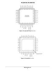
32
1
LQFP−32
FA SUFFIX
CASE 873A
MARKING
DIAGRAM*
XXX = 10 or 100
A = Assembly Location
WL, L = Wafer Lot
YY, Y = Year
WW, W = Work Week
G or G = Pb−Free Package
*For additional marking information, refer to
Application Note AND8002/D.
MCXXX
EP195
AWLYYWWG
http://onsemi.com
See detailed ordering and shipping information in the package
dimensions section on page 17 of this data sheet.
ORDERING INFORMATION
QFN32
MN SUFFIX
CASE 488AM
32
1
MCXXX
EP195
AWLYYWWG
G
1
(Note: Microdot may be in either location)
Verzeichnis
- ・ Konfiguration des Pinbelegungsdiagramms on Seite 3
- ・ Abmessungen des Paketumrisses on Seite 18 Seite 19
- ・ Paket-Footprint-Pad-Layout on Seite 19
- ・ Teilenummerierungssystem on Seite 1 Seite 17 Seite 19
- ・ Markierungsinformationen on Seite 1 Seite 17 Seite 19
- ・ Blockdiagramm on Seite 14
- ・ Typisches Anwendungsschaltbild on Seite 5
- ・ Technische Daten on Seite 17
- ・ Teilenummernliste on Seite 7