

herunterladen

2011-2012 Microchip Technology Inc. Advance Information DS41595B-page 1
PIC12LF1840T48A/T39A
This document includes the
programming specifications for the
following devices:
1.0 OVERVIEW
The PIC12LF1840T48A/T39A is a dual-die device
containing a Microchip PIC12LF1840 microcontroller
and an integrated transmitter. The dies are electrically
isolated.
Since the microcontroller portion of this device is a
standard PIC12LF1840, programming should be done
according to its programming specification,
“PIC16(L)F1847/12(L)F1840 Memory Programming
Specification” (DS41439).
The transmitter contains no user-programmable
memory.
Care should be taken to prevent the transmitter from
transmitting during the programming cycle. In-Circuit
Serial Programming™ (ICSP™) pins should not be
connected to the DATA pin. If the transmitter V
DD
supply is separate from the microcontroller, it should be
kept at V
SS during the programming cycle.
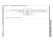
1.1 Pin Utilization
Five pins are needed for ICSP™ programming. Two
additional pins should be connected to ground during
programming. The pins are listed in Table 1-1.
TABLE 1-1: PIN DESCRIPTIONS DURING PROGRAMMING
• PIC12LF1840T48A
• PIC12LF1840T39A
Pin Name
During Programming
Function Pin Type Pin Description
RA1 ICSPCLK I/O Clock Input – Schmitt Trigger Input
RA0 ICSPDAT I/O Data Input/Output – Schmitt Trigger Input
RA3/MCLR
/VPP Program/Verify mode P
(1)
Program mode Select/Programming Power Supply
V
DD VDD P Microcontroller Power Supply
VSS VSS P Microcontroller Ground
VDDRF VDD P RF Power Supply
V
SSRF VSS P RF Ground
Legend: I = Input, O = Output, P = Power
Note 1: The programming high voltage is internally generated. To activate the Program/Verify mode, high voltage
needs to be applied to MCLR
input. Since the MCLR is used for a level source, MCLR does not draw any
significant current.
PIC12LF1840T48A/T39A Programming Specification