
herunterladen

© 2007 Microchip Technology Inc. DS41317B-page 1
PIC16F526
This document includes the
programming specifications for the
following devices:
•PIC16F526
1.0 PROGRAMMING THE
PIC16F526
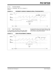
The PIC16F526 is programmed using a serial method.
The Serial mode will allow the PIC16F526 to be pro-
grammed while in the user’s system. This allows for
increased design flexibility. This programming
specification applies to the PIC16F526 devices in all
packages.
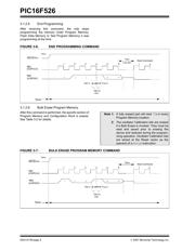
1.1 Hardware Requirements
The PIC16F526 requires one power supply for VDD
(5.0V) and one for VPP (12.5V).
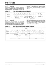
1.2 Program/Verify Mode
The Program/Verify mode for the PIC16F526 allows
programming of user program memory, user ID loca-
tions, backup OSCCAL location and the Configuration
Word.
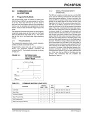
FIGURE 1-1: PIC16F526 14-PIN PDIP, SOIC, TSSOP DIAGRAM
TABLE 1-1: PIN DESCRIPTIONS DURING PROGRAMMING
Pin Name
During Programming
Function Pin Type Pin Description
RB1 ICSPCLK I Clock input – Schmitt Trigger input
RB0 ICSPDAT I/O Data input/output – Schmitt Trigger input
MCLR
/VPP/RB3 Program/Verify mode P
(1)
Programming Power
VDD VDD P Power Supply
V
SS VSS P Ground
Legend: I = Input, O = Output, P = Power
Note 1: In the PIC16F526, the programming high voltage is internally generated. To activate the Program/Verify
mode, high voltage of I
IHH current capability (see Table 6-1) needs to be applied to the MCLR input.
VDD
RB5/OSC1/CLKIN
RB4/OSC2/CLKOUT
RB3/MCLR
/VPP
RC5/T0CKI
RC4/C2OUT
RC3
VSS
RB0/C1IN+/AN0/ICSPDAT
RB1/C1IN-/AN1/ICSPCLK
RB2/C1OUT/AN2
RC0/C2IN+
RC1/C2IN-
RC2/CV
REF
PIC16F526
1
2
3
4
5
6
7
8
9
10
11
12
13
14
PIC16F526 Memory Programming Specification
Verzeichnis