herunterladen
2002 Microchip Technology Inc. DS39025F-page 1
M
PIC16F87X
This document includes the programming
specifications for the following devices:
1.0 PROGRAMMING THE
PIC16F87X
The PIC16F87X is programmed using a serial method.
The Serial mode will allow the PIC16F87X to be pro-
grammed while in the user’s system. This allows for
increased design flexibility. This programming specifi-
cation applies to PIC16F87X devices in all packages.
1.1 Programming Algorithm
Requirements
The programming algorithm used depends on the
operating voltage (V
DD) of the PIC16F87X device.
Algorithm 1 is designed for a V
DD range of
2.2V ≤ V
DD < 5.5V. Algorithm 2 is for a range of
4.5V ≤ V
DD ≤ 5.5V. Either algorithm can be used with
the two available programming entry methods. The first
method follows the normal Microchip Programming
mode entry of applying a V
PP voltage of 13V ± .5V. The
second method, called Low Voltage ICSP
TM
or LVP for
short, applies V
DD to MCLR and uses the I/O pin RB3
to enter Programming mode. When RB3 is driven to
V
DD from ground, the PIC16F87X device enters
Programming mode.
1.2 Programming Mode
The Programming mode for the PIC16F87X allows pro-
gramming of user program memory, data memory, spe-
cial locations used for ID, and the configuration word.
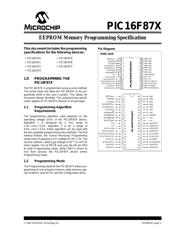
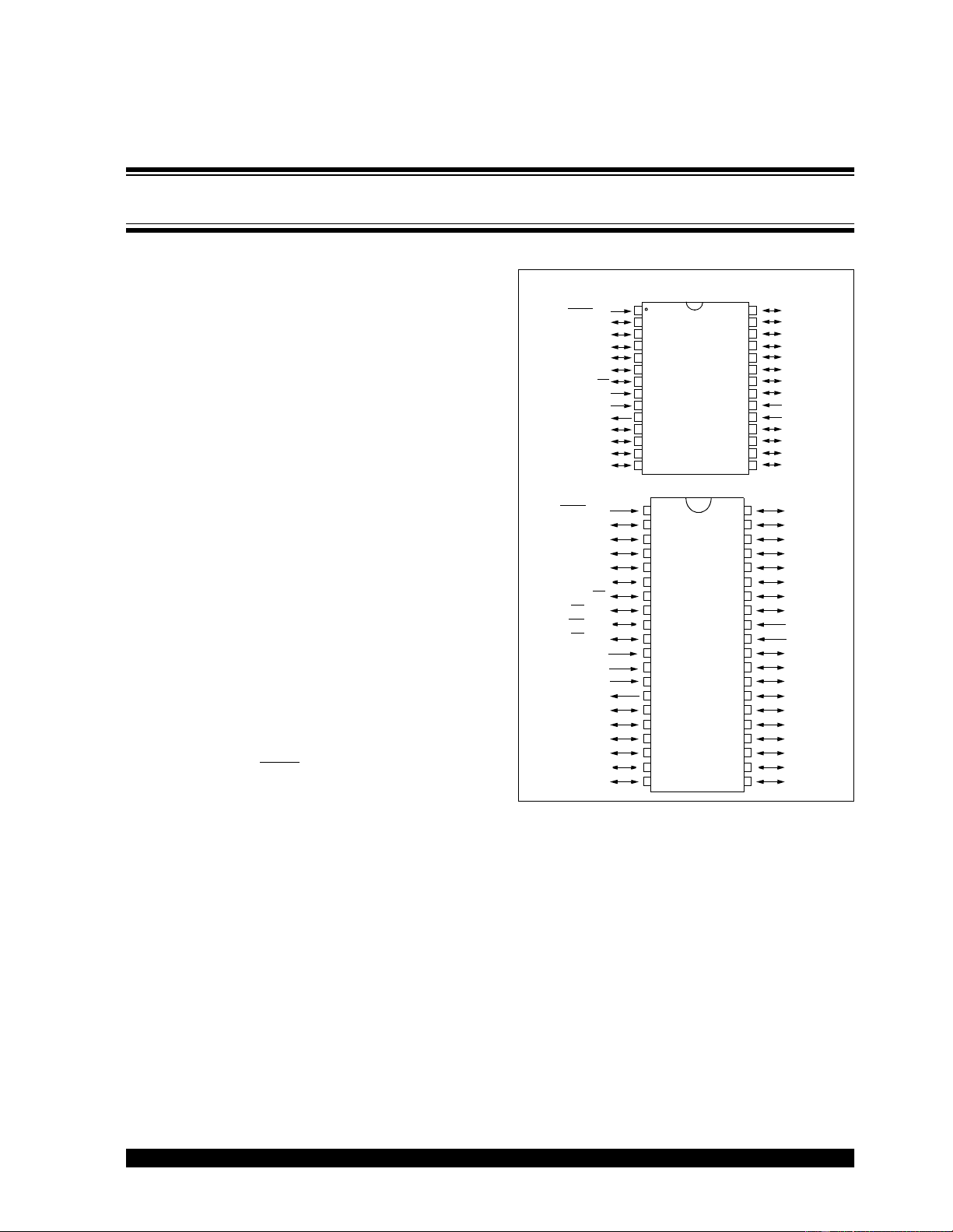
Pin Diagram
•PIC16F870 •PIC16F874
•PIC16F871 •PIC16F876
•PIC16F872 •PIC16F877
•PIC16F873
PDIP, SOIC
RB7
RB6
RB5
RB4
RB3
RB2
RB1
RB0/INT
V
DD
VSS
RD7/PSP7
RD6/PSP6
RD5/PSP5
RD4/PSP4
RC7/RX/DT
RC6/TX/CK
RC5/SDO
RC4/SDI/SDA
RD3/PSP3
RD2/PSP2
MCLR/VPP
RA0/AN0
RA1/AN1
RA2/AN2/VREF
RA3/AN3/VREF
RA4/T0CKI
RA5/AN4/SS
RE0/RD/AN5
RE1/WR/AN6
RE2/CS/AN7
VDD
VSS
OSC1/CLKIN
OSC2/CLKOUT
RC0/T1OSO/T1CKI
RC1/T1OSI/CCP2
RC2/CCP1
RC3/SCK/SCL
RD0/PSP0
RD1/PSP1
1
2
3
4
5
6
7
8
9
10
11
12
13
14
15
16
17
18
19
20
40
39
38
37
36
35
34
33
32
31
30
29
28
27
26
25
24
23
22
21
PIC16F877/874/871
PIC16F876/873/872/870
10
11
2
3
4
5
6
1
8
7
9
12
13
14
15
16
17
18
19
20
23
24
25
26
27
28
22
21
MCLR/VPP
RA0/AN0
RA1/AN1
RA2/AN2/V
REF
RA3/AN3/VREF
RA4/T0CKI
RA5/AN4/SS
VSS
OSC1/CLKIN
OSC2/CLKOUT
RC0/T1OSO/T1CKI
RC1/T1OSI/CCP2
RC2/CCP1
RC3/SCK/SCL
RB7
RB6
RB5
RB4
RB3
RB2
RB1
RB0/INT
V
DD
VSS
RC7/RX/DT
RC6/TX/CK
RC5/SDO
RC4/SDI/SDA
EEPROM Memory Programming Specification
Verzeichnis


