herunterladen
2010 Microchip Technology Inc. Advance Information DS39589C-page 1
PIC16F87XA
This document includes programming
specifications for the following devices:
1.0 PROGRAMMING THE
PIC16F87XA
The PIC16F87XA is programmed using a serial
method. The Serial mode will allow the PIC16F87XA to
be programmed while in the user’s system. This allows
for increased design flexibility. This programming spec-
ification applies to PIC16F87XA devices in all
packages.
1.1 Programming Algorithm
Requirements
The programming algorithm used depends on the
operating voltage (V
DD) of the PIC16F87XA device, or
whether internal or external timing is desired.
Both algorithms can be used with the two available pro-
gramming entry methods. The first method follows the
normal Microchip Programming mode entry of holding
pins RB6 and RB7 low, while raising MCLR
pin from VIL
to VIHH (13V ± 0.5V). The second method, called Low
Voltage ICSP
TM
or LVP for short, applies VDD to MCLR
and uses the I/O pin RB3 to enter Programming mode.
When RB3 is driven to V
DD from ground, the
PIC16F87XA device enters Programming mode.
1.2 Programming Mode
The Programming mode for the PIC16F87XA allows
programming of user program memory, data memory,
special locations used for ID, and the configuration
word.
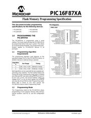
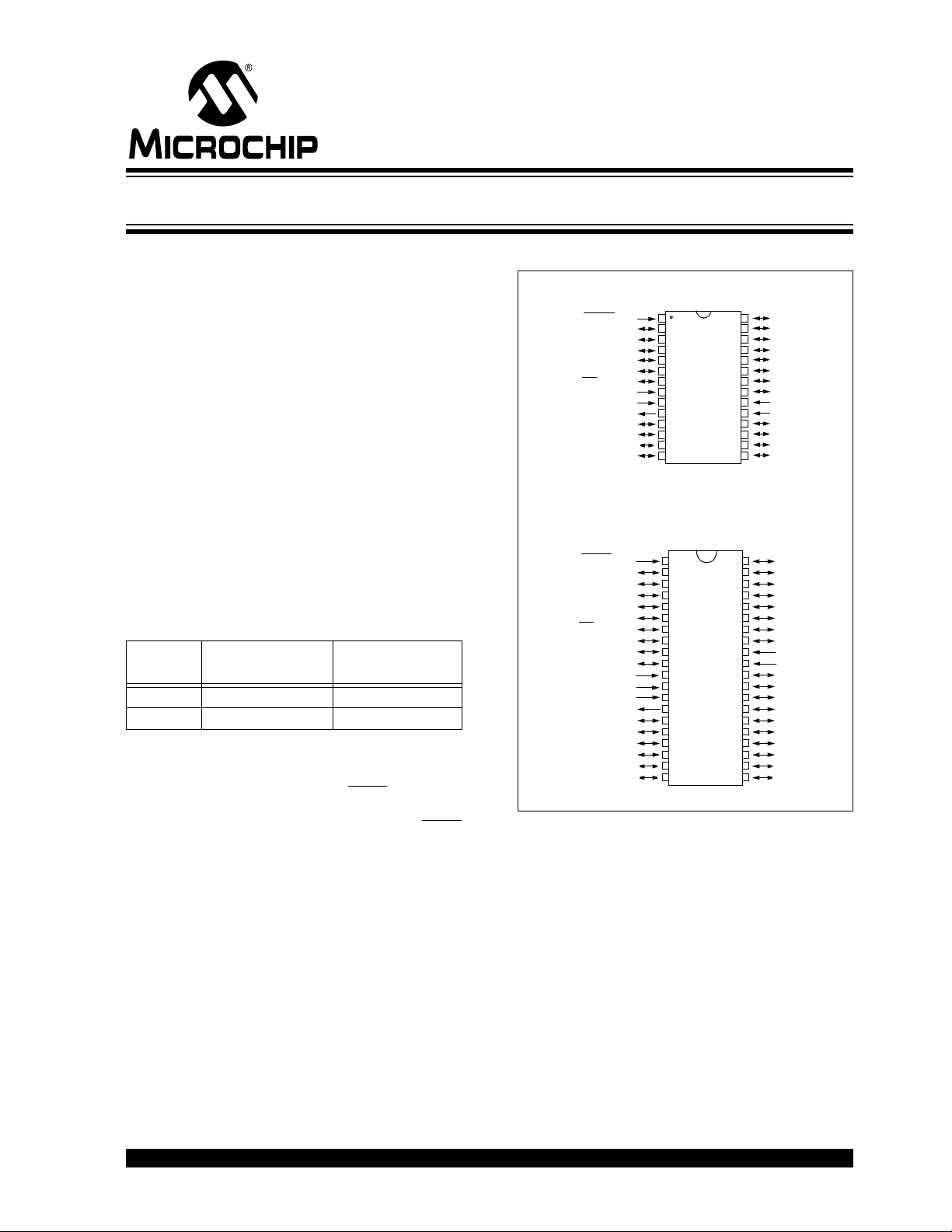
Pin Diagrams
• PIC16F873A • PIC16F876A
• PIC16F874A • PIC16F877A
Algorithm
#
V
DD Range Timing
12.0V V
DD < 5.5V Internal; 4 ms/op
24.5V VDD 5.5V External; 1 ms/op
PDIP, SOIC
PIC16F876A/873A
10
11
2
3
4
5
6
1
8
7
9
12
13
14
15
16
17
18
19
20
23
24
25
26
27
28
22
21
MCLR/VPP
RA0/AN0
RA1/AN1
RA2/AN2/V
REF-/CVREF
RA3/AN3/VREF+
RA4/T0CKI/C1OUT
RA5/AN4/SS
/C2OUT
Vss
OSC1/CLKI
OSC2/CLKO
RC0/T1OSO/T1CKI
RC1/T1OSI/CCP2
RC2/CCP1
RC3/SCK/SCL
RB7/PGD
RB6/PGC
RB5
RB4
RB3/PGM
RB2
RB1
RB0/INT
V
DD
VSS
RC7/RX/DT
RC6/TX/CK
RC5/SDO
RC4/SDI/SDA
RB7/PGD
RB6/PGC
RB5
RB4
RB3/PGM
RB2
RB1
RB0/INT
V
DD
VSS
RD7/PSP7
RD6/PSP6
RD5/PSP5
RD4/PSP4
RC7/RX/DT
RC6/TX/CK
RC5/SDO
RC4/SDI/SDA
RD3/PSP3
RD2/PSP2
MCLR/VPP
RA0/AN0
RA1/AN1
RA2/AN2/V
REF-/CVREF
RA3/AN3/VREF+
RA4/T0CKI/C1OUT
RA5/AN4/SS
/C2OUT
RE0/RD/AN5
RE1/WR/AN6
RE2/CS/AN7
V
DD
VSS
OSC1/CLKI
OSC2/CLKO
RC0/T1OSO/T1CKI
RC1/T1OSI/CCP2
RC2/CCP1
RC3/SCK/SCL
RD0/PSP0
RD1/PSP1
1
2
3
4
5
6
7
8
9
10
11
12
13
14
15
16
17
18
19
20
40
39
38
37
36
35
34
33
32
31
30
29
28
27
26
25
24
23
22
21
PIC16F877A/874A
Flash Memory Programming Specification
Verzeichnis

