herunterladen
© 2009 Microchip Technology Inc. DS41244F-page 1
PIC16F91X/946
This document includes the
programming specifications for the
following devices:
1.0 PROGRAMMING THE
PIC16F91X/946 DEVICES
The PIC16F91X/946 devices are programmed using a
serial method. The Serial mode will allow the PIC16F91X/
946 to be programmed while in the user’s system. This
allows for increased design flexibility. This programming
specification applies to the PIC16F91X/946 devices in all
packages.
1.1 Hardware Requirements
PIC16F91X/946 devices require one power supply for
V
DD and one for VPP (see Section 6.0 “Program/Verify
Mode Electrical Characteristics” for more details).
1.2 Program/Verify Mode
The Program/Verify mode for the PIC16F91X/946
devices allow programming of user program memory,
data memory, user ID locations and the Configuration
Word.
Programming and verification can take place in any
memory region, independent of the remaining regions.
This allows independent programming of program and
data memory regions.
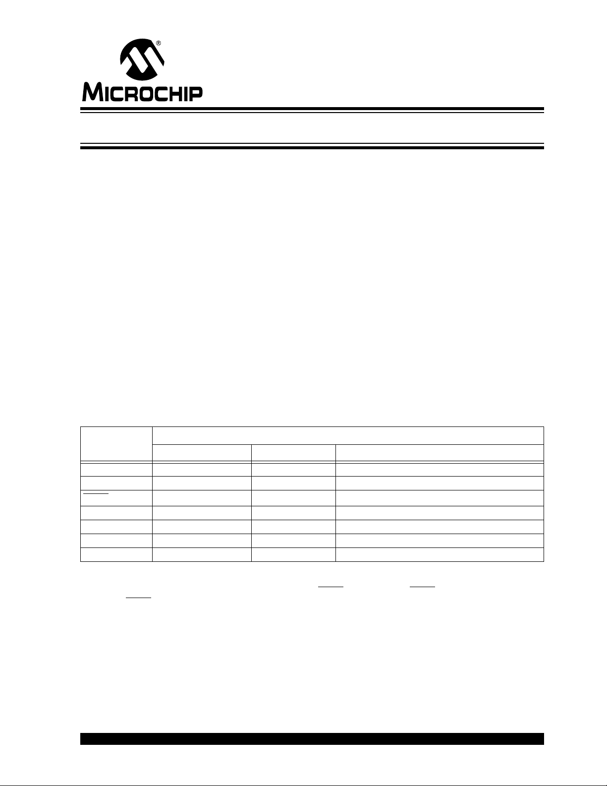
TABLE 1-1: PIN DESCRIPTIONS IN PROGRAM/VERIFY MODE: PIC16F91X/946
•PIC16F913 •PIC16F914 •PIC16F946
•PIC16F916 •PIC16F917
Pin Name
During Programming
Function Pin Type Pin Description
RB6 ICSPCLK I Clock Input – Schmitt Trigger Input
RB7 ICSPDAT I/O Data Input/Output – Schmitt Trigger Input
MCLR
Program/Verify mode P
(1)
Program Mode Select
V
DD VDD P Power Supply
VSS VSS P Ground
AV
DD
(2)
AVDD P Analog Power Supply
AV
SS
(2)
AVSS P Analog Ground
Legend: I = Input, O = Output, P = Power
Note 1: In the PIC16F91X/946, the programming high voltage is internally generated. To activate the Program/
Verify mode, high voltage needs to be applied to MCLR
input. Since the MCLR is used for a level source,
MCLR
does not draw any significant current.
2: AV
DD AND AVSS pins are only available on PIC16F946.
PIC16F91X/946 Memory Programming Specification
Verzeichnis

