

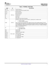
herunterladen
www.ti.com
FEATURES
APPLICATIONS
DESCRIPTION
Flatlink 3Gä
1
4
7
*
3
6
9
#
2
5
8
0
Application
Processor
with
RGB
Video
Interface
LVDS310
LVDS307
M0056-04
LCD
Driver
DATACLK
SN65LVDS310
SLLS836 – MAY 2007
PROGRAMMABLE 27-BIT SERIAL-TO-PARALLEL RECEIVER
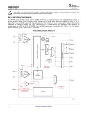
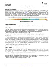
When receiving, the PLL locks to the incoming clock,
CLK, and generates an internal high-speed clock at
• Serial Interface Technology
the line rate of the data lines. The data is serially
• Compatible With FlatLink™ 3G Transmitters
loaded into a shift register using the internal
(E.g., SN65LVDS305 or SN65LVDS307)
high-speed clock. The deserialized data is presented
on the parallel output bus with a recreation of the
• Supports Video Interfaces up to 24-Bit RGB
pixel clock, PCLK, generated from the internal
Data and 3 Control Bits Received Over One
high-speed clock. If no input CLK signal is present,
SubLVDS Differential Data Line
the output bus is held static with PCLK and DE held
• SubLVDS Differential Voltage Levels
low, while all other parallel outputs are pulled high.
• Up to 405-Mbps Data Throughput
The F/S conrol input selects between a slow CMOS
• Three Operating Modes to Conserve Power
bus output rise time for best EMI and power
– Active mode QVGA: 17 mW
consumption and a fast CMOS output for increased
speed or higher-load designs.
– Typical Shutdown: 0.7 µ W
– Typical Standby Mode: 67 µ W Typical
• ESD Rating > 4 kV (HBM)
• Pixel-Clock Range of 4 MHz–15 MHz
• Failsafe on All CMOS Inputs
• Packaged in 4-mm × 4-mm MicroStar
Junior™µ BGA
®
With 0,5-mm Ball Pitch
• Very Low EMI
• Small Low-Emission Interface Between
Graphics Controller and LCD Display
• Mobile Phones and Smart Phones
• Portable Multimedia Players
The SN65LVDS310 receiver deserializes FlatLink
3G-compliant serial input data to 27 parallel data
outputs. The SN65LVDS310 receiver contains one
shift register to load 30 bits from one serial input and
latches the 24 pixel bits and 3 control bits out to the
parallel CMOS outputs after checking the parity bit. If
a parity error is detected, the data output bus
disregards the newly received pixel. Instead, the last
data word is held on the output bus for another clock
cycle.
The serial data and clock are received via
sub-low-voltage differential signalling (SubLVDS)
lines. The SN65LVDS310 supports three operating
power modes (shutdown, standby, and active) to
conserve power.
Please be aware that an important notice concerning availability, standard warranty, and use in critical applications of Texas
Instruments semiconductor products and disclaimers thereto appears at the end of this data sheet.
FlatLink, MicroStar Junior are trademarks of Texas Instruments.
µ BGA is a registered trademark of Tessera, Inc.
PRODUCTION DATA information is current as of publication date.
Copyright © 2007, Texas Instruments Incorporated
Products conform to specifications per the terms of the Texas
Instruments standard warranty. Production processing does not
necessarily include testing of all parameters.
Verzeichnis
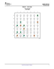
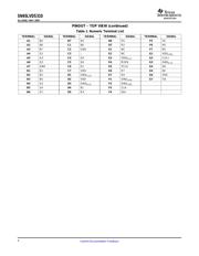
- ・ Abmessungen des Paketumrisses on Seite 28 Seite 29 Seite 30
- ・ Markierungsinformationen on Seite 28
- ・ Blockdiagramm on Seite 2
- ・ Typisches Anwendungsschaltbild on Seite 25
- ・ Beschreibung der Funktionen on Seite 6 Seite 7 Seite 8
- ・ Technische Daten on Seite 9
- ・ Anwendungsbereich on Seite 1 Seite 32
- ・ Elektrische Spezifikation on Seite 11 Seite 12 Seite 21 Seite 22 Seite 23
- ・ Teilenummernliste on Seite 9