

herunterladen
DS026 (v3.9) November 18, 2002 www.xilinx.com 1
Product Specification 1-800-255-7778
© 2001, 2002 Xilinx, Inc. All rights reserved. All Xilinx trademarks, registered trademarks, patents, and further disclaimers are as listed at http://www.xilinx.com/legal.htm. All
other trademarks and registered trademarks are the property of their respective owners. All specifications are subject to change without notice.
NOTICE OF DISCLAIMER: Xilinx is providing this design, code, or information "as is." By providing the design, code, or information as one possible implementation of this feature,
application, or standard, Xilinx makes no representation that this implementation is free from any claims of infringement. You are responsible for obtaining any rights you may
require for your implementation. Xilinx expressly disclaims any warranty whatsoever with respect to the adequacy of the implementation, including but not limited to any warranties
or representations that this implementation is free from claims of infringement and any implied warranties of merchantability or fitness for a particular purpose.
Features
• In-system programmable 3.3V PROMs for
configuration of Xilinx FPGAs
- Endurance of 20,000 program/erase cycles
- Program/erase over full commercial/industrial
voltage and temperature range
• IEEE Std 1149.1 boundary-scan (JTAG) support
• Simple interface to the FPGA
• Cascadable for storing longer or multiple bitstreams
• Low-power advanced CMOS FLASH process
• Dual configuration modes
- Serial Slow/Fast configuration (up to 33 MHz)
- Parallel (up to 264 Mb/s at 33 MHz)
• 5V tolerant I/O pins accept 5V, 3.3V and 2.5V signals
• 3.3V or 2.5V output capability
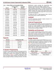
• Available in PC20, SO20, PC44 and VQ44 packages
• Design support using the Xilinx Alliance and
Foundation series software packages.
• JTAG command initiation of standard FPGA
configuration
Description
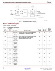
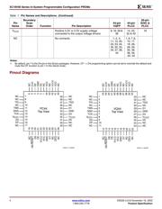
Xilinx introduces the XC18V00 series of in-system program-
mable configuration PROMs (Figure 1). Initial devices in this
3.3V family are a 4-megabit, a 2-megabit, a 1-megabit, a
512-Kbit, and a 256-Kbit PROM that provide an
easy-to-use, cost-effective method for re-programming and
storing large Xilinx FPGA or CPLD configuration bitstreams.
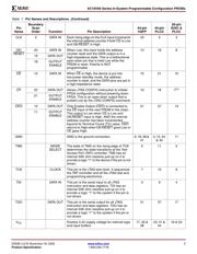
When the FPGA is in Master Serial mode, it generates a
configuration clock that drives the PROM. A short access
time after CE
and OE are enabled, data is available on the
PROM DATA (D0) pin that is connected to the FPGA D
IN
pin. New data is available a short access time after each ris-
ing clock edge. The FPGA generates the appropriate num-
ber of clock pulses to complete the configuration. When the
FPGA is in Slave Serial mode, the PROM and the FPGA are
clocked by an external clock.
When the FPGA is in Master-SelectMAP mode, the FPGA
generates a configuration clock that drives the PROM.
When the FPGA is in Slave-Parallel or Slave-SelectMAP
Mode, an external oscillator generates the configuration
clock that drives the PROM and the FPGA. After CE
and OE
are enabled, data is available on the PROMs DATA (D0-D7)
pins. New data is available a short access time after each
rising clock edge. The data is clocked into the FPGA on the
following rising edge of the CCLK. Neither Slave-Parallel
nor SelectMAP utilize a Length Count, so a free-running
oscillator can be used in the Slave-Parallel or Slave-
SelecMAP modes.
Multiple devices can be concatenated by using the CEO
output to drive the CE input of the following device. The
clock inputs and the DATA outputs of all PROMs in this
chain are interconnected. All devices are compatible and
can be cascaded with other members of the family or with
the XC17V00 one-time programmable Serial PROM family.
0
XC18V00 Series In-System
Programmable Configuration
PROMs
DS026 (v3.9) November 18, 2002
00
Product Specification
R
Verzeichnis