
herunterladen
0 512 1024 1536 2048 2560 3072 3584 4096
Code
0.5
0.4
0.3
0.2
0.1
0
–0.1
–0.2
–0.3
–0.4
–0.5
DLE Error (LSB)
0 512 1024 1536 2048 2560 3072 3584 4096
Code
0.5
0.4
0.3
0.2
0.1
0
–0.1
–0.2
–0.3
–0.4
–0.5
DLE Error (LSB)
Application Report
SBAA052A–October 2000–Revised May 2015
Analog-to-Digital Converter Grounding Practices Affect
System Performance
................................................................................................................... High-PerformanceAnalog
ABSTRACT
Obtaining optimum performance from a high-resolution analog-to-digital converter (ADC) depends upon
many factors. Power supply decoupling and good grounding practices are essential to maintaining
accuracy in ADCs.
Poor grounding technique may manifest itself in many different ways such as excessive noise, or signal
crosstalk in the system. A more difficult problem to track down is that of poor differential linearity error
(DLE) in the converter. This is difficult because poor DLE may result from settling time problems inside the
ADC, from the circuitry driving the ADC having too high an output impedance at the converter’s operating
frequency, from poor grounding techniques or other sources.
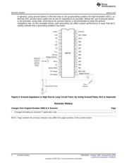
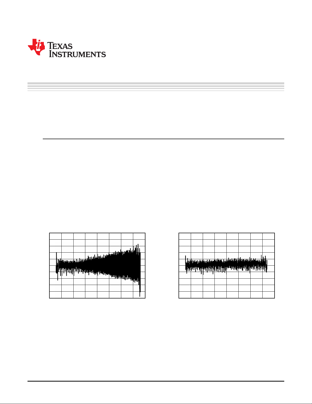
Figure 1 is a DLE plot of a ADCTH (12-bit, 8μs conversion time ADC) in a specific printed circuit board.
This histogram plots deviation from ideal differential linearity against specific codes output from the
converter. The circuit shown in Figure 1 has a DLE of about ±0.4LSB. This meets the specification of the
ADC774, but is less than optimum.
The cause of the DLE performance is the grounding scheme used in this application. The part was
“grounded” using recommendations made in most of our ADC data sheets: connect the analog and digital
grounds together at the ADC.
Figure 1. ADC774 Board DLE with Poor Ground Figure 2. ADC774 Board DLE with Improved Ground.
What went wrong is that the analog and digital commons were connected together at the ADC, but that
“ground” was then returned through a long trace on the PCB to the system ground. This means that the
“ground” the ADC actually saw had a fair amount of resistance and inductance, as shown in Figure 3.
Returning the analog and digital common of the same ADC to a single ground plane underneath the
converter (Figure 3) reduced this inductance and resistance considerably, and thus made the ADC “see” a
much lower impedance; a more optimum ground. The results of this improved grounding technique are
shown in Figure 2. The new board exhibits a DLE of only about ±0.1LSB, much closer to what the
ADC774 typically does.
1
SBAA052A–October 2000–Revised May 2015 Analog-to-Digital Converter Grounding Practices Affect System Performance
Submit Documentation Feedback
Copyright © 2000–2015, Texas Instruments Incorporated