
herunterladen
© Semiconductor Components Industries, LLC, 2014
November, 2014 − Rev. 6
1 Publication Order Number:
BUV26/D
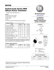
BUV26
Switch‐mode Series NPN
Silicon Power Transistor
Designed for high−speed applications.
Features
• Switch-mode Power Supplies
• High Frequency Converters
• Relay Drivers
• Driver
• These Devices are Pb−Free and are RoHS Compliant*
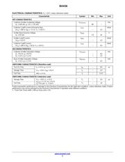
MAXIMUM RATINGS (T
J
= 25°C unless otherwise noted)
Rating
Symbol Value Unit
Collector−Emitter Voltage V
CEO(sus)
90 Vdc
Collector−Base Voltage V
CBO
180 Vdc
Emitter−Base Voltage V
EBO
7.0 Vdc
Collector Current − Continuous I
C
20 Adc
Collector Current − Peak (pw 10 ms) I
CM
30 Adc
Base Current − Continuous I
B
4.0 Adc
Base Current − Peak I
BM
6.0 Adc
Total Power Dissipation @ T
C
= 25°C
Total Power Dissipation @ T
C
= 60°C
P
D
P
D
85
65
W
W
Operating and Storage Junction
Temperature Range
T
J
, T
stg
− 65 to +175
°C
Stresses exceeding those listed in the Maximum Ratings table may damage the
device. If any of these limits are exceeded, device functionality should not be
assumed, damage may occur and reliability may be affected.
THERMAL CHARACTERISTICS
Characteristic Symbol Max Unit
Thermal Resistance,
Junction−to−Case
R
q
JC
1.76 °C/W
*For additional information on our Pb−Free strategy and soldering details, please
download the ON Semiconductor Soldering and Mounting Techniques
Reference Manual, SOLDERRM/D.
Device Package Shipping
ORDERING INFORMATION
12 AMPERES
NPN SILICON
POWER TRANSISTORS
90 VOLTS, 85 WATTS
MARKING
DIAGRAM
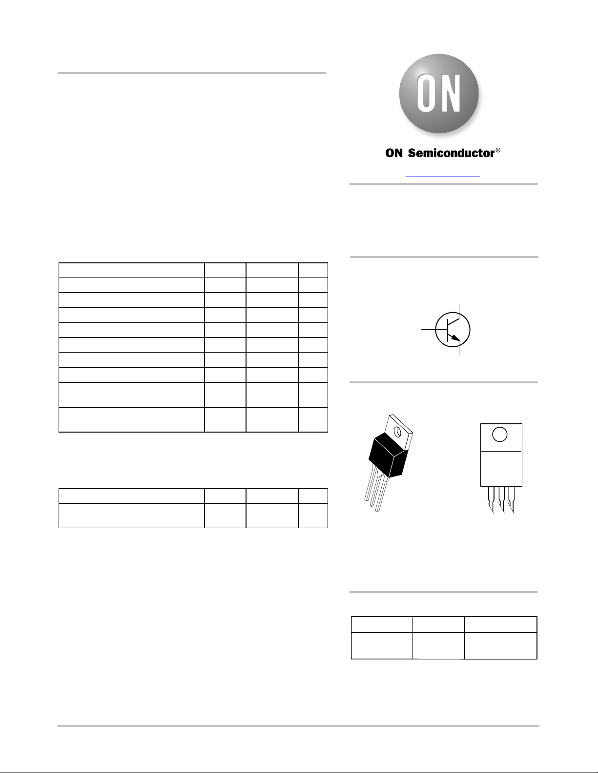
www.onsemi.com
BUV26G
TO−220
(Pb−Free)
50 Units / Rail
BUV26 = Device Code
A = Assembly Location
Y = Year
WW = Work Week
G = Pb−Free Package
BUV26G
AYWW
TO−220
CASE 221A
STYLE 1
1
2
3
4
1
1
BASE
3
EMITTER
COLLECTOR
2,4
SCHEMATIC
Verzeichnis