
herunterladen
© Semiconductor Components Industries, LLC, 2013
April, 2013 − Rev. 3
1 Publication Order Number:
CM1451/D
CM1451
LCD and Camera EMI Filter
Array with ESD Protection
Description
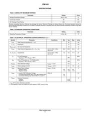
The CM1451 is an inductor−capacitor (L−C) based EMI filter array
with integrated ESD protection in CSP. The CM1451−06 and
CM1451−08 are configured in 6 and 8 channel formats respectively.
Each channel is implemented as a 5−pole L−C filter with the
component values 9.5 pF − 17 nH − 9.5 pF − 17 nF − 9.5 pF. The
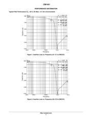
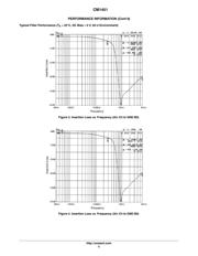
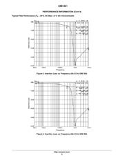
CM1451’s roll−off frequency at −10 dB attenuation is 500 MHz. It can
be used in applications where the data rates are as high as 200 Mbps
while providing greater than 35 dB attenuation over the 800 MHz to
2.7 GHz frequency range. The device has ESD protection diodes on
every pin that provide a very high level of protection for sensitive
electronic components that may be subjected to electrostatic discharge
(ESD). The ESD protection diodes connected to the filter ports safely
dissipate ESD strikes of ±15 kV, exceeding the Level 4 requirement of
the IEC61000−4−2 international standard. Using the MIL−STD−883
(Method 3015) specification for Human Body Model (HBM) ESD, the
pins are protected for contact discharges at greater than ±30 kV.
This device is particularly well−suited for portable electronics (e.g.
wireless handsets, PDAs) because of its small package format and
easy−to−use pin assignments. In particular, the CM1451 is ideal for
EMI filtering and protecting data and control lines for the LCD display
and camera interface in wireless handsets while maintaining the
integrity of signals that have rise/fall times as fast as 2 ns.
The CM1451 incorporates OptiGuard, a coating that results in
improved reliability at assembly. The CM1451 is available in a
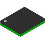
space−saving, low−profile Chip Scale Package with RoHS compliant
lead−free finishing.
Features
• High Bandwidth, High RF Rejection Filter Array
• Six and Eight Channels of EMI Filtering
• Utilizes Inductor−Based Design Technology for True L−C Filter
Implementation
• OptiGuard Coating for Improved Reliability
• Chip Scale Package (CSP) Features Extremely Low Lead
Inductance for Optimum Filter and ESD Performance
• 15 kV ESD Protection on Each Channel
(IEC 61000−4−2 Level 4, Contact Discharge)
• 30 kV ESD Protection on Each Channel (HBM)
• Better than 40 dB of Attenuation at 1 GHz
• Maintains Signal Integrity for Signals that Have a
Risetime and Falltime as Fast as 2 ns
• 15−Bump, 3.006 mm x 1.376 mm Footprint Chip Scale
Package (CM1451−06CP)
• 20−Bump, 4.006 mm x 1.376 mm Footprint Chip Scale
Package (CM1451−08CP)
• These Devices are Pb−Free and are RoHS Compliant
Applications
• LCD and Camera Data Lines in Mobile Handsets
• I/O Port Protection for Mobile Handsets, Notebook
Computers, PDAs, etc.
• Wireless Handsets / Cell Phones
• EMI Filtering for Data Ports in Cell Phones, PDAs or
Notebook Computers
• Handheld PCs / PDAs
• LCD and Camera Modules
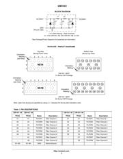
MARKING DIAGRAM
Device Package Shipping
†
ORDERING INFORMATION
http://onsemi.com
CM1451−06CP CSP−15
(Pb−Free)
3500/Tape & Reel
N516 = CM1451−06CP
N518 = CM1451−08CP
N516
CM1451−08CP CSP−20
(Pb−Free)
3500/Tape & Reel
CM1451−06
15−Bump CSP Package
N518
CM1451−08
20−Bump CSP Package
†For information on tape and reel specifications,
including part orientation and tape sizes, please
refer to our Tape and Reel Packaging Specification
Brochure, BRD8011/D.
WLCSP15
CP SUFFIX
CASE 567BT
WLCSP20
CP SUFFIX
CASE 567CL
Verzeichnis
- ・ Konfiguration des Pinbelegungsdiagramms on Seite 2
- ・ Abmessungen des Paketumrisses on Seite 9 Seite 10
- ・ Paket-Footprint-Pad-Layout on Seite 9 Seite 10
- ・ Teilenummerierungssystem on Seite 1 Seite 10
- ・ Markierungsinformationen on Seite 1 Seite 2 Seite 10
- ・ Blockdiagramm on Seite 2
- ・ Schweißen Temperatur on Seite 8
- ・ Technische Daten on Seite 3
- ・ Anwendungsbereich on Seite 1